Push-Pull Class B Transistor Power-Output Circuits
|
|
The fundamentals of class-B push-pull amplifiers have not changed since 1960 when this article appeared in Electronics World magazine. The transistors for making them have improved in most cases, but the design procedures are basically the same. Class-B amplifiers, in case you are not familiar with the topology, are able to amplify zero-referenced sinusoidal signals throughout the full 360 degrees of rotation signals without an offset voltage bias; they are constructed from two class-A amplifiers in a cascode configuration. Issues like crossover distortion and thermal runaway are discussed in the amplifier design procedure. Here is the class A transistor amplifier article. Push-Pull Class B Transistor Power-Output Circuits  By Walter H. Buchsbaum / Industrial Consultant,
Electronics World By Walter H. Buchsbaum / Industrial Consultant,
Electronics World
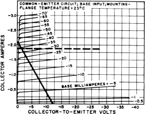
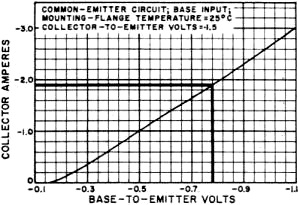
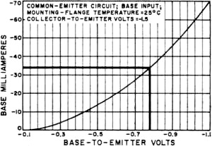
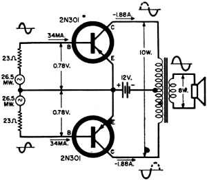
Simple design procedure that will help to understand this very useful and popular transistorized circuitry. Transistor audio amplifiers have many advantages over their vacuum-tube counterparts, but one circuit that really highlights these advantages is the Class B push-pull power amplifier. The great efficiency and simplicity of transistors really shine in this application. With no filament power required and a relatively low "B+" voltage, the power drain during quiet periods is negligible and the overall circuit efficiency extremely high. These are certainly very desirable features. Another attraction is the price of germanium power transistors which compares favorably with vacuum tubes. In this article a typical 8-watt amplifier design, which uses transistors costing about $3.00 each, will be illustrated. The same design procedure can be used for amplifiers at other power levels and for different transistor types. Those readers who are more concerned with troubleshooting transistor audio amplifiers will find the material helpful in understanding the sources of the most frequent defects they are apt to find in transistor circuits. Class B operation means that each transistor will amplify only one-half of the signal and will "rest" while its mate amplifies the opposite-polarity portion of the signal. Because power dissipation is one of the most critical factors in transistors, Class B operation is particularly suited to the task of insuring low dissipation for each transistor. There are only two drawbacks to this type of transistor circuit: crossover distortion and thermal runaway. These will be discussed below. Crossover distortion occurs when one transistor stops conducting before the other has started and is a typical problem with all Class B circuits. Thermal runaway can occur in any transistor application but power transistors are especially susceptible. This trouble is due to the fact that, as a transistor heats up, it will tend to draw more current which, in turn, will cause the collector to heat up even more until the unit burns out. There are well-established and relatively simple cures for both crossover distortion and thermal runaway and they will be described here in some detail. Let us first consider the characteristic curves. Most of our readers will be somewhat familiar with the characteristic curves used in vacuum-tube circuit design. Similar curves are furnished by transistor manufacturers and are used in the same manner. In last month's article on Class A transistor power-output circuits we described some of the special aspects of transistor characteristic curves, a discussion which will not be repeated here. Instead, we will concentrate on the design of a typical amplifier and point out how crossover distortion, thermal runaway, and some of the minor problems can be handled. Amplifier Design Procedure In any power amplifier design the governing factors will be the desired power output, available voltage, and component efficiency. Assuming that we wish to be able to deliver 8 watts to the loudspeaker, we must first account for the losses in the output transformer, which may be about 80 percent efficient. This immediately brings the actual maximum power that the two transistors must deliver up to about 10 watts. If we want to allow for 25 percent overload capacity, the power is increased to 12.5 watts or 6.25 watts per transistor. A typical supply voltage would be 12 volts which would permit operating the equipment direct from an automobile battery or two 6-volt lantern batteries. It would also be possible to build a well regulated supply, using a standard 12.6-volt filament transformer as power source. Once the power and the voltage are determined, we can select a transistor type. It must be able to handle at least 6.25 watts and must have a collector-to-emitter voltage rating of at least twice the supply voltage, which means 24 volts. For our example we have selected the 2N301 which is made by RCA, Bendix, Sylvania, and CBS, and is readily available at parts distributors. This transistor is rated at 40 volts collector potential and can dissipate 11 watts at 80°C which means about 25 watts at room temperature. These ratings are higher than our minimum requirements but they afford us a much needed margin of safety. To get an idea of what the peak-current swing per stage can be, we can calculate: 6.25 watts x (4 ¸ 12) volts = 2.1 amps The manufacturers' data shows that the 2N301 can handle up to 3 amps. peak current. To get the load resistance per stage we divide the 12-volt supply voltage by the 2.1 amp. peak current and this is roughly 6 ohms. One of the characteristics of Class B push-pull circuits is the fact that the total primary impedance of the output transformer is four times the load resistance per stage or 24 ohms in our example. Fig. 1 - Collector characteristics of 2N301. Fig. 2 - Transfer characteristics of 2N301. Fig. 3 - Base characteristics of the 2N301. Fig. 4 - Basic design of the 8·watt amplifier.
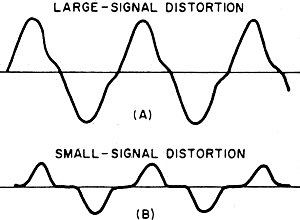
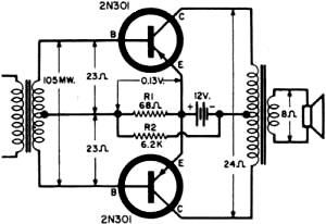
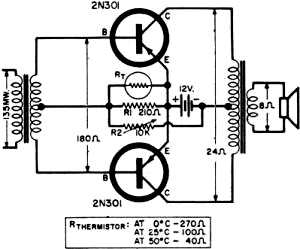
Fig. 5 - The distortion due to the crossover. Fig. 6 - Pre-bias circuit for the amplifier. At this point it is useful to study the characteristic curves of the transistor in question. Fig. 1 shows the collector characteristics for the 2N301 for various values of base current. The a.c. load line for the 6-ohm load resistance is drawn by connecting the 12-volt, zero-current point to the 2.1-amp., zero-voltage point. To calculate maximum power handling ability we have accounted for 25 percent overload capacity, but for normal operation the current and voltage swing will be limited by a factor: k = sqrt (1/1.25) = 0.896 Therefore, the normal full-load current swing will be only 2.1 amp. x 0.896 = 1.88 amp., as shown by the dotted line in Fig. 1. Another curve, Fig. 2, shows the average transfer characteristic which is simply a plot of collector current vs base voltage. For 1.88 amps. of collector current, the base voltage will have to be 0.78 volt and this, on the base characteristic curve of Fig. 3, will cause a base current of 34 ma. The product of 34 ma. x 0.78 volt is the input power, 26.5 mw. The input impedance per transistor can be found by Ohm's Law from 0.78 volt divided by 34 ma., or 23 ohms. We can now draw a basic diagram of the Class B amplifier with its input and output requirements, as shown in Fig. 4. This simple circuit will, however, suffer from the disadvantages inherent in Class B transistor amplifiers. If we drive this amplifier with a sine-wave signal of maximum amplitude, 0.78 volt peak at the base of each stage, then the output signal at the loudspeaker will have the waveform of Fig. 5A, which shows the typical symptoms of crossover distortion. Crossover Distortion Fig. 5 illustrates one of the most frequent defects in Class B transistor amplifiers and the technician working with these circuits will soon become quite familiar with the appearance of these distorted output signals, To understand the cause for crossover distortion we need only look at the average transfer characteristic curve of Fig. 2 and study the lower portion of the curve below 0.2 volt of base bias. Here the curve flattens out and stops completely at 0.13 volt. This means that from about zero to 0.13 volt of base signal, no current flows in the collector circuit. When the base signal is very small the collector signal will take the form of the curve of Fig. 5B, with current flowing only during that portion of the sine wave which corresponds to more than 0.13 volt of base voltage. Since the two push-pull transistors have the same characteristics, the distortion will be balanced about the zero line of the sine-wave signal. To overcome this trouble it will be necessary to pre-bias each transistor slightly. In effect, for small signals, the transistors then operate as Class A amplifiers. This method can completely eliminate crossover distortion but it means that each transistor draws some current at all times and this reduces the efficiency of the Class B stages. In a good design, the pre-bias voltage is set carefully to minimize the quiescent collector current. Returning to the design of Fig. 4, we can see two places where a pre-bias might be inserted. We could insert an additional battery between ground and the two emitters or, and this is the simpler approach, we can utilize a portion of the 12-volt collector supply to bleed a small negative voltage to the two bases. This will cause a loss in input signal due to the impedance or the biasing network. In a circuit of this type the bias resistors cannot be bypassed because the capacitor would charge up to the signal voltage level and this would increase the fixed bias too much. The 2N301 characteristic curves of Figs. 2 and 3 indicate that a pre-bias of about - 0.13 volt is required. Previously we calculated the peak input impedance to be about 23 ohms. The bias resistor should usually be about three times as large so we select a value of 68 ohms, a readily available and standard unit. By using Ohm's Law we find the current through the resistor to be 1.91 ma. At 0.13 volt the base current itself is practically zero so that only about 2 ma. will flow in the bias resistor. Because of the variations among individual transistors and other circuit constants, it is advisable to include a potentiometer in the bias voltage divider and set the actual voltage level for minimum collector current, commensurate with minimum crossover distortion. Looking at the revised circuit of Fig. 6, we can now see that the input power of 26.5 mw. which we calculated previously will not be sufficient because the actual input impedance, per stage, is not now 23 ohms but a total of 91 ohms. The ratio between the I2R input power for equal current is simply the ratio of 23 and 91 ohms, which is 3.95. This corresponds to approximately 6 db, the increase in input needed to overcome the effect of the pre-biasing network. The input power required to drive the circuit of Fig. 6 for peak output is, therefore, 105 mw. Accounting for transformer losses of 20 percent, we find that the actual peak driving power delivered by a driver amplifier to the primary of the input transformer will have to be about 135 mw. Driving circuits for Class B power amplifiers deserve a lengthy article in themselves, but in this limited space we can only point out that Class A single-stage amplifiers or Class A push-pull circuits are usually used in this application. There are a number of circuits which avoid the use of a driving transformer and provide phase splitting and impedance matching directly. For the example cited here it would be possible to use a single-stage Class A 2N301 as driver or else a Type 2N32, 2N44, or 2N226, all suitable and readily available from jobber stocks. The prime requirement of a driver stage is power handling ability. If the reader refers to last month's article on Class A power amplifiers, all of the circuit designs can be followed except that the Class B push-pull stage input impedance must be substituted for the load on the output transformer secondary. Thermal Runaway One of the basic facts about semiconductor physics is the interdependence of current flow and temperature. As the temperature goes up, more current flows. As current flows, heat is generated in the transistor. These two facts impose a severe restriction on the circuit designer, especially when germanium transistors are used where the critical temperatures are relatively close to room temperature. Silicon devices have a somewhat higher critical temperature. The transistor characteristic curves of Figs. 1, 2, and 3 all bear the notation "mounting flange temperature 25°C" and this means that at a higher or lower temperature the characteristics shown may be changed somewhat. If a transistor were 100 percent efficient it would have no power loss in the transistor itself but such a device is, of course, unavailable. The2N301, according to the published data, will dissipate 3 watts for an output of 12 watts in a Class B push-pull circuit. The 3 watts of heat must be conducted away from the transistor or else it will build up to a progressively higher temperature. If the flange temperature increases, the current through the collector increases and the amount of power which is dissipated in the transistor also increases. In other words, if the mounting arrangement of the transistor cannot dissipate 3 watts of power, the resulting temperature build-up will burn out the transistor. It is possible, by careful design, to mount each transistor so that it can easily radiate 3 watts into the surrounding air, but on a hot day the efficiency of this heat transfer will suffer because the surrounding air itself is warmer. In last month's article on Class A power amplifiers we illustrated several techniques for mounting power transistors for maximum heat radiation. The same approach should be used for Class B push-pull circuits except that we must be careful not to allow the heat from one transistor to contribute to the other, unless the dissipation from both can be radiated readily. In addition to the mechanical mounting methods, there are simple electronic means of preventing thermal runaway and maintaining stability with varying temperatures. The most widely used method involves base bias control by means of a temperature-sensitive resistor or "thermistor." A thermistor can either increase or decrease in resistance with temperature, but the latter type is more common. In using a thermistor to control the bias of a transistor the thermistor is mounted close to the transistor heat sink so that any heat rise in the transistor will affect the resistance of the thermistor. Returning once again to our example of a typical Class B push-pull circuit we can see how a thermistor is used in the circuit of Fig. 7. Here the thermistor, RT, part of the bias network and in parallel with the 210-ohm carbon resistor, provides the desired 68 ohms at 25°C. When the temperature increases to 50°C the thermistor will be only 40 ohms and this will reduce the pre-bias enough to cut the transistor collector current down to a safe value. The principle is simply to reduce bias as temperature goes up and to do this in conformity with the transistor characteristics. If the right thermistor were used, the fixed resistance R1 would not be required, but most commercially available thermistors are more temperature sensitive than needed and therefore a fixed shunting resistor is often used. Transformer Considerations Before we can build the final circuit of Fig. 7, we must give some thought to the two transformers. These items must be selected from available stock types and, if a perfect match is not possible, the effects of mismatch will have to be evaluated. Starting at the output stage, we immediately know that this transformer will have to be the bigger one since it must handle at least 8 watts. Actually a 10-watt unit will be the standard size. In checking through the catalogue we find that a number of manufacturers make suitable units of this type. To cite just one, consider the Triad TY-29X. It has a center-tapped primary with an impedance of 24 ohms and a secondary with either 8- or 4-ohm impedances. It can handle 10 watts of audio power. We can see that it meets our requirements exactly. There are a number of other transformers equally suitable, such as the Stancor T-14 or Chicago TAMS-12. It may happen that in another design the calculated output impedance turns out to be a value which cannot be matched by a commercial output transformer. We can then use the nearest available transformer type or change the design of our circuit. The first method is recommended when the nearest available transformer impedance is not more than 25 percent higher than the transistor output impedance. Otherwise it is possible to change the output impedance by redrawing the load line. We can change either the supply voltage or the peak power and, if necessary, select a different transistor type. When we consider the input transformer we see that, as far as the Class B amplifier is concerned, we can select only the secondary and the power ratings. In our example the input transformer must be capable of handling at least 135 mw. and must match the input impedance of 182 ohms. Actually, to minimize distortion, the source impedance should be lower than the input impedance so we should select a transformer which has less than 182 ohms secondary impedance. A good choice would be the Thordarson TR64 which has a 100-ohm center-tapped secondary and a primary impedance of 100 ohms. It can handle 0.5 watt which is ample for this circuit. Because the secondary impedance is lower, some loss in power transfer will occur here which means that the driver stage will have to deliver more than the 135 mw. previously calculated. In a conservative design the driver stage will be capable of delivering at least twice the driving power calculated for the Class B output stages. Conclusion Class B transistor amplifiers have the great advantage of requiring almost no quiescent power and are, therefore, very efficient. The design principles are the same as for vacuum-tube push-pull Class B circuits, except that the transistor's temperature characteristics must be taken into account. The detailed design procedure presented here requires only a knowledge of Ohm's Law, arithmetic, and an understanding of characteristics curves.
Posted October 8, 2021 |
|

