Class A Transistor Power-Output Circuits
|
|
One of the first things you learn in school when studying transistors is the three classes of amplifier circuits: Class A, where the conduction angle is a full 360°; Class B, where the conduction angle is 180°; and Class C, where the conduction angle is less than 180°. There is a fourth hybrid Class AB, which conducts more than 180° but less than 360°. Class A is generally considered the simplest configuration to produce a linear operation, where the output signal is exactly the same multiple in voltage as the input signal. For example if the gain of the amplifier is 100, then a 0.01 V input produces a 1 V output, a 0.1 V input produces a 10 V output, and a 1 V input produces a 100 V output. Perfect linearity produces no distortion in the output, with no spectral components not present in the input. Why wouldn't you want to use a Class A amplifier all the time, you might ask? The answer is that it is the least efficient configuration. In order to conduct through a full 360°, a DC bias is required to place the output halfway between the maximum peak-to-peak output voltage so that the transistor is never turned fully on or fully off. That means with no input signal or a less than maximum input signal, the amplifier is turned on at least half-way and therefore is dissipating more power than necessary. That being said, there are applications where a Class A amplifier is useful, such as driving a local oscillator input to a mixer, where the amplitude is constant and the circuit can be optimized for the known, constant output level. Here is the class B transistor amplifier article. Class A Transistor Power-Output Circuits
Some simple, as well as useful, basic circuit-design information that will help to understand class A transistor output circuits. Among the many possible transistor power-amplifier circuits two basic types are certain to be included in any list of preferred or standard circuits. One is the class A single-stage output amplifier and the second is the class B push-pull circuit. These two circuits can be used with practically any power transistor on the market and can be designed for almost any amount of output power, linearity, frequency response, etc. This article will consider the operation of class A transistor power amplifiers and will present sufficient engineering detail to permit the reader to design an amplifier, tailor-made to his own special requirements. Commercially available amplifiers are designed by the same process and an understanding of the technique will be of help in repairing such equipment. Transistor Characteristics
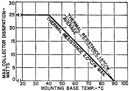
Fig. 1 - Power-derating curve of 2N235A.
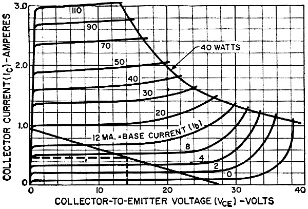
Fig. 2 - Collector characteristics of 2N176.
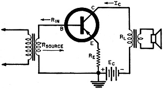
Fig. 3 - Grounded-emitter output amplifier.
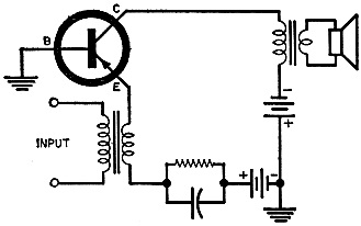
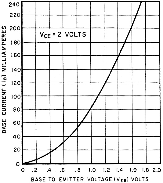
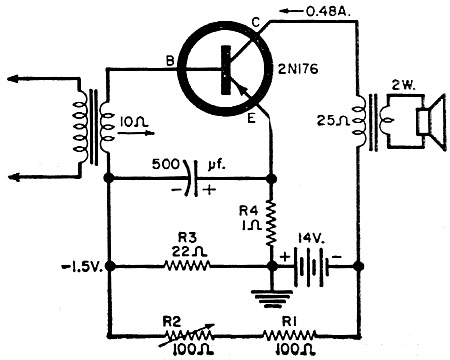
Fig. 4 - A grounded base output amplifier. Just as tube characteristics are important in the design or troubleshooting of vacuum-tube circuits, transistor characteristics must similarly be understood first. We assume that our readers are somewhat familiar with vacuum-tube characteristic curves and therefore we proceed to compare them to transistor characteristics. The first factor which must be considered in selecting a transistor as a power amplifier is its power handling ability. Vacuum tubes are rated according to maximum plate dissipation, without any reference to operating temperatures. Transistors, however, are rated according to maximum collector dissipation at a certain temperature, usually 25°C, which corresponds to approximately 75°F or room temperature. If the maximum power is dissipated in the transistor, the temperature of the transistor itself will rise and this will limit its power handling ability. A transistor capable of handling 10 watts at 25°C sometimes can handle only 3 watts at 50°C. This brings us to the first important transistor characteristic which is different from its vacuum-tube counterpart. This is the power derating curve, a typical example of which is shown in Fig. 1. On the vertical axis we read the maximum collector dissipation in watts and on the horizontal axis the mounting base temperature is plotted. Fig. 1 applies to the type 2N235A which is a 25-watt transistor, similar to the 2N301 and a number of others. Note that up to 40°C of mounting base temperature the maximum collector dissipation of 25 watts is permissible, but as the mounting temperature goes up less power can be handled by the collector. At 90°C, with zero collector dissipation, the mounting temperature and the transistor junction temperature are the same. The solid line of Fig. 1 is based on the worst conditions, while the dotted line is representative of average transistor variations. To be on the safe side the designer should stay within the left portion of the solid line. More detail on temperature control is given in a later paragraph. The other important transistor characteristics can be compared to their vacuum-tube equivalents. First comes the output characteristic which shows collector current versus collector volt-age and, as apparent from the example of Fig. 2, this is equivalent to the plate characteristics of tubes. Instead of grid voltage, base current is used here as parameter but, the load line and other design features are obtained just as for vacuum-tube amplifiers .. The constant dissipation contour shown in Fig. 2, is similar to maximum plate-dissipation curves supplied for power-output tubes. Transistor input characteristics are comparable to the grid curves supplied for vacuum tubes, except that the base-current versus base-voltage curves are not usually as linear as grid curves. A third type of characteristic, which is usually supplied with transistor data, is the transfer characteristic which shows collector-current output versus base-current input at a fixed collector voltage. This curve is very useful in determining linearity and bias. Having convinced ourselves that transistor characteristic curves are no more complex than those which we have used for vacuum-tube circuits, we can now examine the operation of a class A transistor output amplifier. Operating Features Class A operation means that the output waveform will be a facsimile of the input signal and this means that the transistor will conduct during the entire cycle. To obtain proper linearity, the collector voltage and current must vary over a linear portion of the output characteristics. In transistor amplifier design it is possible to ground the base, the collector, or the emitter, with each connection having certain advantages and drawbacks. For audio power amplifiers the most frequently used connection is the one shown in Fig. 3 in which the emitter is effectively grounded. This provides the greatest amount of power gain while still giving reasonable linearity. Fig. 4 shows the connection for grounded-base amplifier, a circuit which gives excellent linearity but less power gain than the grounded-emitter scheme. The third connection has the collector grounded for a.c. and is called an emitter-follower. Like the cathode-follower this third circuit has high input and low output impedance, but is not really an amplifier. It is not usually used as class A single-stage and will therefore not be considered here. One of the features of any class A power stage, tube or transistor, is the fact that considerable power is dissipated during zero-signal conditions. In a transistor this means that the quiescent point must be chosen well below the maximum collector dissipation and therefore the full power handling ability of the transistor cannot be used. The battery or power supply must deliver considerable power during zero-signal conditions. For these reasons class A amplifiers are not usually used for large power output stages, but are limited to applications below 5 watts. When two transistors are used in class A push-pull, the standby power requirement remains, but each transistor can be driven harder and all even-harmonic distortions are cancelled out. Considerable second-and third-harmonic distortion can be encountered in single-stage class A amplifiers, but careful design and certain precautions can keep distortion below 5%. Class A Amplifier Design Some texts treat transistor circuit design in great detail and involve the use of accurate mathematical expressions. In this article, however, only simple arithmetic is required to design certain basic amplifier circuits from manufacturers' data. Approximations, simplifications, and certain basic assumptions are made about the transformers and other parts, which are available from jobbers' shelves, The design procedures may not be accurate enough for servo amplifiers used in missile guidance systems, but they will do for practical audio amplifiers, that our technically minded readers can design, build, and work with. A practical approach to the design of a typical class A power amplifier must start with the known requirements. How much audio power should be produced? What battery or power-supply voltage is available? In this example the desired output power might be 2 watts. Assuming that the output trans-former efficiency is 75% we can see at once that the amplifier itself must de-liver 2.67 watts in order to drive the speaker with 2 watts. Next we must provide for some overload capacity, say 25%, and this increases the power output capability of the transistor stage to 3.35 watts. Adding at least 3.35 watts for d.c. dissipation we can see that the collector dissipation must be at least 6.7 watts. If we choose a nominal battery voltage of 14 volts, the collector current can be calculated from Ohm's Law as: Ic = 6.7 watts/14 volts = 0.48 amp. Similarly, the load resistance is: RL = 14 volts/048 amp. = 29 ohms (approx.) Now we can select a transistor by knowing that it must have a collector dissipation of over 6.7 watts and be able to stand a peak-inverse voltage swing of at least 2 times 14 or 28 volts. One such transistor is the 2N176, available from most jobbers and manufactured by RCA, Sylvania, Motorola, among others. The 2N176 collector can dissipate 10 watts and has a peak-inverse voltage rating of 40 volts, a safe margin for our requirements. The manufacturer's data for the type 2N176 transistor includes the collector characteristics which are shown in Fig. 2. We locate the intersection of 14 volts and 0.48 amp., which is then the quiescent point, just as in vacuum-tube circuits. The load line is drawn by connecting the quiescent point with the 28-volt point on the base line or the 0.96-amp. point on the vertical axis. A look at the load-line drawing of Fig. 2 will indicate some of the reasons for non-linearity in the output signals. The quiescent point is here set for a base current of approximately 6 ma. A swing from 0 to 12 ma. would result in an output voltage swing from 25 to 8 volts, and this would produce a sine wave in which one portion is compressed as compared with the other The base current is, of course, determined by the base voltage and by the signal source impedance. By making the source impedance much smaller than the base input impedance and by providing some bias on the base itself this non-linearity can be compensated for to some extent. We see from Fig: 2 that the maximum base current will be approximately 20 ma. Next we refer to the input characteristic curve of Fig. 5 which shows that approximately 0.5 volt of base signal would be required to produce 20 ma. of base current. Multiplying these two figures we obtain the required maximum input power which is 10 mw. The input impedance can be approximated, using Ohm's Law: 0.5 volt/0.020 amp. = 25 ohms To reduce distortion we can choose a source impedance of 10 ohms. The power gain of the stage can be calculated from the ratio of output power to input power, which, in this example, is 267. This corresponds to a power gain of approximately 24 db. To get an approximate idea of the value of the emitter resistor, we .must determine the base voltage at the quiescent point which is approximately 0.25 volt. Using Ohm's Law again we know that the quiescent collector current of 0.48 amp. must pass through this emitter resistor and we then obtain a value for it as follows: 0.25 volt/0.48 amp. = 1/2 ohm It is a safe assumption that a 1-ohm resistor in the emitter circuit will be approximately correct. If we want to determine the circuit efficiency of our class A amplifier we divide the audio output power, 2.67 watts, by the total input power, 6.7 watts, and multiply the results by 100 to obtain approximately 40%. We have now established all of the values for the circuit of Fig. 3 and from this we can go to the practical circuit which is shown in Fig. 6. Note that in this circuit we have added a forward bias of approximately 1.5 volts which is applied to the base through the voltage divider R1 R2 and R3. Some circuits use a separate battery, usually located in the emitter lead, but for simplicity's sake a voltage divider has been used in Fig. 6. The adjustable resistor is set for best output linearity. A 500-μf. bypass capacitor is used between the emitter and the input transformer winding to keep a.c. out of the bias circuit. The 1-ohm emitter resistor limits the emitter current and therefore the base bias can effectively shift the quiescent point on the load line to obtain more linear output without causing excessive collector current to flow. It is possible to obtain 2 watts of audio power with a maximum of 3% distortion over a frequency range from 60 cps to 10 kc. with this circuit. Some of the loss at the higher frequencies is compensated by the increased efficiency of both transformers. The circuit shown in Fig. 6 and the design procedure described above is applicable to other transistor types as well. In many instances manufacturing data includes some of the values calculated here and occasionally a complete circuit diagram for a class A audio amplifier is provided as part of the data sheets. Controlling Temperature
Fig. 5 - Input characteristics of 2N176.
Fig. 6 - A practical class A circuit.
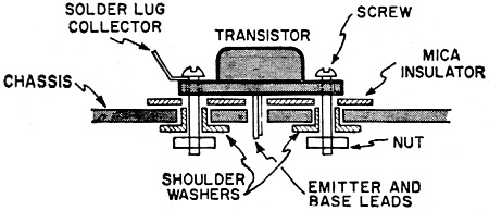
Fig. 7 - Chassis mounting of transistor.
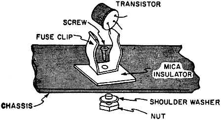
Fig. 8 - The fuse-clip heat sink.
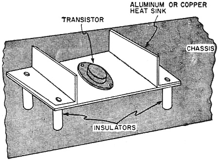
Fig. 9 - Elaborate insulated heat sink.
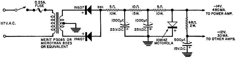
Fig. 10 - Typical power-supply circuit schematic. As pointed out earlier, one of the limitations of any transistor is its sensitivity to changes in temperature. When the transistor gets warmer, more collector current can flow, which, in turn, tends to make it warmer still. This is often called "thermal runaway" and is the prime transistor killer in experimental work. Sometimes a circuit works perfectly until a hot day comes along and then things seem to go haywire. There are several safeguards against thermal runaway and one of them has already been included in the design just discussed. This safeguard is the emitter resistor which at least limits the collector current and provides a back bias as the collector current in-creases. Another safeguard is the original circuit design which centers around a power range well below the maximum for that particular transistor. In Fig. 2 we can see that the load line chosen is well removed from the 40-watt maximum dissipation curve. Actually the collector temperature at the maximum design power level of 6.7 watts could go. up beyond the room temperature of 25°C, but to play it safe we have designed for that temperature. If we were to operate this circuit at, say, 60°C, then we would have to provide some temperature compensation such as a thermistor, connected across the 22-ohm leg of the base-biasing circuit. As temperature increases, resistance of the thermistor drops and this also reduces the forward bias and therefore tends to limit collector current. Aside from the problems introduced by thermal runaway and possible higher ambient temperatures, collector dissipation must be considered. All power transistors have the collector connected directly to the outside body and depend on dissipating collector power through the body. For this reason it is usually necessary to mount a power transistor on some kind of heat sink. In our previous example, over 3 watts of d.c. power is dissipated in the collector. If no heat sink is provided this power will quickly heat up the transistor body, raise the internal temperature, and thereby increase the collector current. Even with a suitable emitter resistor, the thermal runaway effect could take over. It is absolutely necessary that the collector power be dissipated into the surrounding air and, in most Instances, the transistor case itself cannot radiate heat fast enough. There are many different ways of helping the transistor dissipate heat. Some power transistors are available with tight fitting copper radiating bodies and fins. Others can be mounted on specially designed heat sinks. Almost all power transistors are sold with a mica or alumina oxide mounting washer which permits mounting the transistor on the chassis for heat dissipation while obtaining electrical insulation. A typical arrangement is shown in Fig. 7. Ordinary insulators cannot be used since they do a poor job of transmitting heat. In locating power transistors on a chassis we must make certain that the heat they contribute does not injure other transistors and that the chassis is reasonably cool to begin with. In addition to radiating the heat on the chassis itself, some home-made auxiliary heat sinks can be used. A simple fuse clip or capacitor mounting clip can be used, especially on smaller power transistors, as shown in Fig. 8. The clip should make contact with the transistor body in as many places as possible to allow heat transfer to the clip. While the illustration shows the clip mounted against the chassis through a mica washer arrangement, in low-power applications the clip can be insulated by regular Bakelite or cardboard and then only the clip radiates the heat. For larger power transistors the arrangement of Fig. 9 is quite useful. A rectangular sheet of aluminum, copper, or brass is used and, to add radiating surface, two angle pieces are bolted on each end. The entire structure can be mounted on Bakelite or ceramic stand-offs which provide electrical insulation from the chassis. To further increase heat radiation, any of the heat sinks can be painted black, but care must be taken that the heat transfer points be-tween the transistor and the heat sink are not covered with paint. One frequent mistake made by people unfamiliar with transistors is that they forget to make an electrical connection to the body of the transistor which is the collector. Never solder to the transistor body since this is equivalent to heating the entire unit. A solder lug should be screwed on to the unpainted mounting flange and the wire should, preferably, be soldered to the lug beforehand. Power Supply or Battery Our readers may justly wonder about a suitable source of 14 volts at half an ampere. Batteries that can deliver such power are rather large, and smaller units don't last very long. The ordinary laboratory type power supplies can deliver the power but not at the voltage and current required. For this reason special power supplies are usually designed to work with transistor circuits. While there is not enough space in this article for a complete description of such supplies, we do want to give the reader some idea of what is required. The circuit shown in Fig. 10 is typical of those used with transistor audio amplifiers and has certain features which make it somewhat different from vacuum-tube type supplies. The power transformer is available from jobber's stock and is widely used for selenium-rectifier, low-voltage supplies. Although two 1N607 rectifiers are shown, any unit capable of 500-ma., 50-volt peak inverse operation will do. The reason for not using a choke is that chokes having low enough d.c. resistance are not always available. Capacitors of the values shown are readily available and the power resistors are also carried in jobber's stock. One luxury accessory in the power supply of Fig. 10 is the zener diode, type 10M14Z. It is not absolutely necessary but Will help to reduce a.c. ripple, voltage variations with load changes, and will also present a low output impedance for the power supply. The author has found that the addition of a zener diode greatly improves over-all amplifier performance and is well worth the extra expense. Conclusion The basic method for designing a class A transistor power amplifier has been explained and a typical design has been illustrated. Class A operation, especially with transistors, is not very efficient for larger power ranges, and a number of precautions must be observed. Distortion can be reduced by proper circuit design and selection of a very low signal-source impedance. The heat generated by the collector current must be dissipated to avoid overheating of the transistor. To supply the low voltage and relatively high current, a fairly simple power supply can be constructed and a circuit for such a unit is shown here. Despite some of the disadvantages of using a class A power output amplifier, the circuit simplicity and reliable operation make this circuit useful in many low-power applications.
Posted May 16, 2023 |
|