Module 7 - Introduction to Solid-State Devices and Power Supplies |
||||||||||||||||||||||||||||||||||||||||||||||||||
|
Module 7 − Introduction to Solid−State Devices and Power Supplies
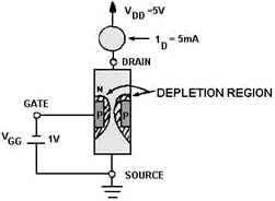
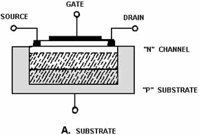
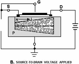
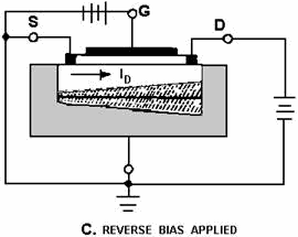
Pages i , 1−1, 1−11, 1−21, 1−31, 1−41, 2−1, 2−11, 2−21, 2−31, 2−41, 2−51, 3−1, 3−11, 3−21, 3−31, 3−41, 3−51, 4−1 to 4−10, 4−11, 4−21, 4−31, 4−41, 4−51, Index "depletion region" to form around the PN junction of the JFET. Because this region has a reduced number of current carriers, the effect of reverse biasing is to reduce the effective cross-sectional area of the "channel." This reduction in area increases the source-to-drain resistance of the device and decreases current flow.
Figure 3-48. - JFET with reverse bias.
The application of a large enough negative voltage to the gate will cause the depletion region to become so large that conduction of current through the bar stops altogether. The voltage required to reduce drain current (ID) to zero is called "pinch-off" voltage and is comparable to "cut-off" voltage in a vacuum tube. In figure 3-48, the negative 1 volt applied, although not large enough to completely stop conduction, has caused the drain current to decrease markedly (from 10 milliamperes under zero gate bias conditions to 5 milliamperes). Calculation shows that the 1-volt gate bias has also increased the resistance of the JFET (from 500 ohms to 1 kilohm). In other words, a 1-volt change in gate voltage has doubled the resistance of the device and cut current flow in half.
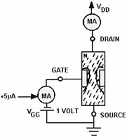
These measurements, however, show only that a JFET operates in a manner similar to a bipolar transistor, even though the two are constructed differently. As stated before, the main advantage of an FET is that its input impedance is significantly higher than that of a bipolar transistor. The higher input impedance of the JFET under reverse gate bias conditions can be seen by connecting a microammeter in series with the gate-source voltage (VGG), as shown in figure 3-49.
3-41
Figure 3-49. - JFET input impedance.
With a VGG of 1 volt, the microammeter reads .5 microamps. Applying Ohm's law (1V ÷ .5 µA) illustrates that this very small amount of current flow results in a very high input impedance (about 2 megohms). By contrast, a bipolar transistor in similar circumstances would require higher current flow (e.g., .1 to -1 mA), resulting in a much lower input impedance (about 1000 ohms or less). The higher input impedance of the JFET is possible because of the way reverse-bias gate voltage affects the cross- sectional area of the channel.
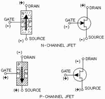
The preceding example of JFET operation uses an N-channel JFET. However, a P-channel JFET operates on identical principles. The differences between the two types are shown in figure 3-50.
Figure 3-50. - JFET symbols and bias voltages.
Because the materials used to make the bar and the gate are reversed, source voltage potentials must also be reversed. The P-channel JFET therefore requires a positive gate voltage to be reverse biased, and current flows through it from drain to source.
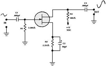
3-42 Figure 3-51 shows a basic common-source amplifier circuit containing an N-channel JFET. The characteristics of this circuit include high input impedance and a high voltage gain. The function of the circuit components in this figure is very similar to those in a triode vacuum tube common-cathode amplifier circuit. C1 and C3 are the input and output coupling capacitors. R1 is the gate return resistor and functions much like the grid return resistor in a vacuum tube circuit. It prevents unwanted charge buildup on the gate by providing a discharge path for C1. R2 and C2 provide source self-bias for the JFET, which operates like cathode self-bias. R3 is the drain load resistor, which acts like the plate or collector load resistor.
Figure 3-51. - JFET common source amplifier.
The phase shift of 180 degrees between input and output signals is the same as that of common- cathode vacuum tube circuits (and common-emitter transistor circuits). The reason for the phase shift can be seen easily by observing the operation of the N-channel JFET. On the positive alternation of the input signal, the amount of reverse bias on the P-type gate material is reduced, thus increasing the effective cross-sectional area of the channel and decreasing source-to-drain resistance. When resistance decreases, current flow through the JFET increases. This increase causes the voltage drop across R3 to increase, which in turn causes the drain voltage to decrease. On the negative alternation of the cycle, the amount of reverse bias on the gate of the JFET is increased and the action of the circuit is reversed. The result is an output signal, which is an amplified 180-degree-out-of-phase version of the input signal.
a second type of field-effect transistor has been introduced in recent years that has some advantages over the JFET. This device is the metal oxide semiconductor field effect transistor (MOSFET). The MOSFET has an even higher input impedance than the JFET (10 to 100 million megohms). Therefore, the MOSFET is even less of a load on preceding circuits. The extremely high input impedance, combined with a high gain factor, makes the MOSFET a highly efficient input device for RF/IF amplifiers and mixers and for many types of test equipment.
The MOSFET is normally constructed so that it operates in one of two basic modes: the depletion mode or the enhancement mode. The depletion mode MOSFET has a heavily doped channel and uses reverse bias on the gate to cause a depletion of current carriers in the channel. The JFET also operates in this manner. The enhancement mode MOSFET has a lightly doped channel and uses forward bias to
3-43 enhance the current carriers in the channel. a MOSFET can be constructed that will operate in either mode depending upon what type of bias is applied, thus allowing a greater range of input signals.
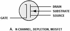
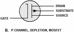
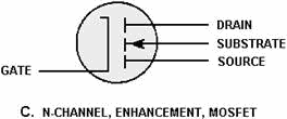
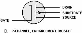
In addition to the two basic modes of operation, the MOSFET, like the JFET, is of either the P-channel type or the N-channel type. Each type has four elements: gate, source, drain, and substrate. The schematic symbols for the four basic variations of the MOSFET are shown in views A, B, C, and D of figure 3-52.
Figure 3-52A. - MOSFET symbols.
Figure 3-52B. - MOSFET symbols.
Figure 3-52C. - MOSFET symbols.
3-44
Figure 3-52D. - MOSFET symbols.
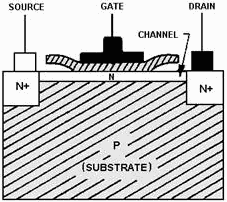
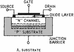
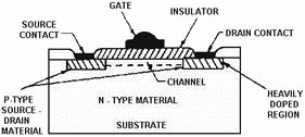
The construction of an N-channel MOSFET is shown in figure 3-53. Heavily doped N-type regions (indicated by the N+) are diffused into a P-type substrate or base. a channel of regular N-type material is diffused between the heavily doped N-type regions. a metal oxide insulating layer is then formed over the channel, and a metal gate layer is deposited over the insulating layer. There is no electrical connection between the gate and the rest of the device. This construction method results in the extremely high input impedance of the MOSFET. Another common name for the device, derived from the construction method, is the insulated gate field effect transistor (IGFET).
Figure 3-53. - MOSFET structure.
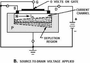
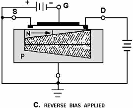
The operation of the MOSFET, or IGFET, is basically the same as the operation of the JFET. The current flow between the source and drain can be controlled by using either of two methods or by using a combination of the two methods. In one method the drain voltage controls the current when the gate potential is at zero volts. a voltage is applied to the gate in the second method. An electric field is formed by the gate voltage that affects the current flow in the channel by either depleting or enhancing the number of current carriers available. As previously stated, a reverse bias applied to the gate depletes the carriers, and a forward bias enhances the carriers. The polarity of the voltages required to forward or reverse bias a MOSFET depends upon whether it is of the P-channel type or the N-channel type. The effects of reverse-bias voltage on a MOSFET designed to operate in the depletion mode are illustrated in
3-45 views A, B, and C of figure 3-54. The amount of reverse bias applied has a direct effect on the width of the current channel and, thus, the amount of drain current (ID).
Figure 3-54A. - Effects of bias on N-channel depletion MOSFET.
Figure 3-54B. - Effects of bias on N-channel depletion MOSFET. 3-46
Figure 3-54C. - Effects of bias on N-channel depletion MOSFET.
Figure 3-55 (view A, view B, and view C) illustrates the effect of forward bias on an enhancement mode N-channel MOSFET. In this case, a positive voltage applied to the gate increases the width of the current channel and the amount of drain current (ID).
Figure 3-55A. - Effects of bias on N-channel enhancement MOSFET. 3-47
Figure 3-55B. - Effects of bias on N-channel enhancement MOSFET.
Figure 3-55C. - Effects of bias on N-channel enhancement MOSFET.
Another type of MOSFET is the induced-channel type MOSFET. Unlike the MOSFETs discussed so far, the induced-channel type has no actual channel between the source and the drain. The induced channel MOSFET is constructed by making the channel of the same type material as the substrate, or the opposite of the source and the drain material. As shown in figure 3-56, the source and the drain are of P-type material, and the channel and the substrate are of N-type material.
3-48
Figure 3-56. - Induced channel MOSFET construction.
The induced-channel MOSFET is caused to conduct from source to drain by the electric field that is created when a voltage is applied to the gate. For example, assume that a negative voltage is applied to the MOSFET in figure 3-56. The effect of the negative voltage modifies the conditions in the substrate material. As the gate builds a negative charge, free electrons are repelled, forming a depletion region. Once a certain level of depletion has occurred (determined by the composition of the substrate material), any additional gate bias attracts positive holes to the surface of the substrate. When enough holes have accumulated at the surface channel area, the channel changes from an N-type material to a P-type material, since it now has more positive carriers than negative carriers. At this point the channel is considered to be to inverted, and the two P-type regions at the source and the drain are now connected by a P-type inversion layer or channel. As with the MOSFET, the gate signal determines the amount of current flow through the channel as long as the source and drain voltages remain constant. When the gate voltage is at zero, essentially no current flows since a gate voltage is required to form a channel.
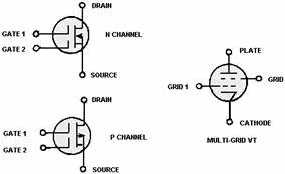
The MOSFETs discussed up to this point have been single-gate MOSFETs. Another type of MOSFET, the dual-gate type, is shown in figure 3-57. As the figure shows, the gates in a dual-gate MOSFET can be compared to the grids in a multi-grid vacuum tube. Because the substrate has been connected directly to the source terminal, the dual-gate MOSFET still has only four leads: one each for source and drain, and two for the gates. Either gate can control conduction independently, making this type of MOSFET a truly versatile device.
Figure 3-57. - Dual-gate MOSFET.
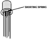
3-49 One problem with both the single- and dual-gate MOSFETs is that the oxide layer between gate and channel can be destroyed very easily by ordinary static electricity. Replacement MOSFETs come packaged with their leads shorted together by a special wire loop or spring to avoid accidental damage. The rule to remember with these shorting springs is that they must not be removed until after the MOSFET has been soldered or plugged into a circuit. One such spring is shown in figure 3-58.
Figure 3-58. - MOSFET shorting spring.
Q30. What is one of the primary advantages of the FET when compared to the bipolar transistor?
Q31. The FET and the vacuum tube have what in common?
Q32. The base of a transistor serves a purpose similar to what element of the FET?
Q33. What are the two types of JFET?
Q34. The source and drain of an N-channel JFET are made of what type of material?
Q35. What is the key to FET operation?
Q36. What is the normal current path in an N-channel JFET?
Q37. Applying a reverse bias to the gate of an FET has what effect?
Q38. The input and output signals of a JFET amplifier have what phase relationship?
Q39. When compared to the JFET, what is the input impedance of the MOSFET?
Q40. What are the four elements of the MOSFET?
Q41. The substrate of an N-channel MOSFET is made of what material?
Q42. In a MOSFET, which element is insulated from the channel material?
Q43. What type of MOSFET can be independently controlled by two separate signals?
Q44. What is the purpose of the spring or wire around the leads of a new MOSFET?
3-50
|
||||||||||||||||||||||||||||||||||||||||||||||||||