Module 7 - Introduction to Solid-State Devices and Power Supplies
|
||||||||||||||||||||||||||||||||||||||||||||||||||
|
Module 7 − Introduction to Solid−State Devices and Power Supplies
Pages i , 1−1, 1−11, 1−21, 1−31, 1−41, 2−1, 2−11, 2−21, 2−31, 2−41, 2−51, 3−1, 3−11, 3−21, 3−31, 3−41, 3−51, 4−1 to 4−10, 4−11, 4−21, 4−31, 4−41, 4−51, Index
Chapter 2
Transistors Learning Objectives Upon completion of this chapter, you should be able to do the following: 1. Define the term transistor and give a brief description of its construction and operation. 2. Explain how the transistor can be used to amplify a signal. 3. Name the four classes of amplifiers and give an explanation for each. 4. List the three different transistor circuit configurations and explain their operation. 5. Identify the different types of transistors by their symbology and alphanumerical designations. 6. List the precautions to be taken when working with transistors and describe ways to test them. 7. Explain the meaning of the expression "integrated circuits." 8. Give a brief description on how integrated circuits are constructed and the advantages they offer over conventional transistor circuits. 9. Name the two types of circuit boards. 10. State the purpose and function of modular circuitry. Introduction to Transistors
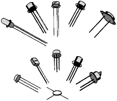
Figure 2-1 - An assortment of different types of transistors. The discovery of the first transistor in 1948 by a team of physicists at the Bell Telephone Laboratories sparked an interest in solid-state research that spread rapidly. The transistor, which began as a simple laboratory oddity, was rapidly developed into a semiconductor device of major importance. The transistor demonstrated for the first time in history that amplification in solids was possible. Before the transistor, amplification was achieved only with electron tubes. Transistors now perform numerous electronic tasks with new and improved transistor designs being continually put on the market. In many cases, transistors are more desirable than tubes because they are small, rugged, require no filament power, and operate at low voltages with comparatively high efficiency. The development of a family of transistors has even made possible the miniaturization of electronic circuits. Figure 2-1 shows a sample of the many different types of transistors you may encounter when working with electronic equipment. Transistors have infiltrated virtually every area of science and industry, from the family car to satellites. Even the military depends heavily on transistors. The ever increasing uses for transistors have created an urgent need for sound and basic information regarding their operation. From your study of the PN-junction diode in the preceding chapter, you now have the basic knowledge to grasp the principles of transistor operation. In this chapter you will first become acquainted with the basic types of transistors, their construction, and their theory of operation. You will also find out just how and why transistors amplify. Once this basic information is understood, transistor terminology, capabilities, limitations, and identification will be discussed. Last, we will talk about transistor maintenance, integrated circuits, circuit boards, and modular circuitry. Transistor Fundamentals The first solid-state device discussed was the two-element semiconductor diode. The next device on our list is even more unique. It not only has one more element than the diode but it can amplify as well. Semiconductor devices that have-three or more elements are called Transistors. The term transistor was derived from the words transfer and resistor. This term was adopted because it best describes the operation of the transistor - the transfer of an input signal current from a low-resistance circuit to a high-resistance circuit. Basically, the transistor is a solid-state device that amplifies by controlling the flow of current carriers through its semiconductor materials. There are many different types of transistors, but their basic theory of operation is all the same. As a matter of fact, the theory we will be using to explain the operation of a transistor is the same theory used earlier with the PN-junction diode except that now two such junctions are required to form the three elements of a transistor. The three elements of the two-junction transistor are (1) the Emitter, which gives off, or emits," current carriers (electrons or holes); (2) the Base, which controls the flow of current carriers; and (3) the Collector, which collects the current carriers. Classification
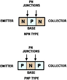
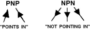
Figure 2-2 - Transistor block diagrams. Transistors are classified as either NPN or PNP according to the arrangement of their N and P materials. Their basic construction and chemical treatment is implied by their names, "NPN" or "PNP." That is, an NPN transistor is formed by introducing a thin region of P-type material between two regions of N-type material. On the other hand, a PNP transistor is formed by introducing a thin region of N-type material between two regions of P-type material. Transistors constructed in this manner have two PN junctions, as shown in figure 2-2. One PN junction is between the emitter and the base; the other PN junction is between the collector and the base. The two junctions share one section of semiconductor material so that the transistor actually consists of three elements. Since the majority and minority current carriers are different for N and P materials, it stands to reason that the internal operation of the NPN and PNP transistors will also be different. The theory of operation of the NPN and PNP transistors will be discussed separately in the next few paragraphs. Any additional information about the PN junction will be given as the theory of transistor operation is developed. To prepare you for the forthcoming information, the two basic types of transistors along with their circuit symbols are shown in figure 2-3. It should be noted that the two symbols are different. The horizontal line represents the base, the angular line with the arrow on it represents the emitter, and the other angular line represents the collector. The direction of the arrow on the emitter distinguishes the NPN from the PNP transistor. If the arrow points in, (Points In) the transistor is a PNP. On the other hand if the arrow points out, the transistor is an NPN (Not Pointing iN). Another point you should keep in mind is that the arrow always points in the direction of hole flow, or from the P to N sections, no matter whether the P section is the emitter or base. On the other hand, electron flow is always toward or against the arrow, just like in the junction diode. Construction
Figure 2-3 - Transistor representations.
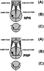
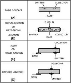
Figure 2-4 - Transistor constructions. The very first transistors were known as point-contact transistors. Their construction is similar to the construction of the point-contact diode covered in chapter 1. The difference, of course, is that the point-contact transistor has two P or N regions formed instead of one. Each of the two regions constitutes an electrode (element) of the transistor. One is named the emitter and the other is named the collector, as shown in figure 2-4, view A. Point-contact transistors are now practically obsolete. They have been replaced by junction transistors, which are superior to point-contact transistors in nearly all respects. The junction transistor generates less noise, handles more power, provides higher current and voltage gains, and can be mass-produced more cheaply than the point-contact transistor. Junction transistors are manufactured in much the same manner as the PN junction diode discussed earlier. However, when the PNP or NPN material is grown (view B), the impurity mixing process must be reversed twice to obtain the two junctions required in a transistor. Likewise, when the alloy-junction (view C) or the diffused-junction (view D) process is used, two junctions must also be created within the crystal. Although there are numerous ways to manufacture transistors, one of the most important parts of any manufacturing process is quality control. Without good quality control, many transistors would prove unreliable because the construction and processing of a transistor govern its thermal ratings, stability, and electrical characteristics. Even though there are many variations in the transistor manufacturing processes, certain structural techniques, which yield good reliability and long life, are common to all processes: (1) Wire leads are connected to each semiconductor electrode; (2) the crystal is specially mounted to protect it against mechanical damage; and (3) the unit is sealed to prevent harmful contamination of the crystal. Q1. What is the name given to the semiconductor device that has three or more elements? Q2. What electronic function made the transistor famous? Q3. In which direction does the arrow point on an NPN transistor? Q4. What was the name of the very first transistor? Q5. What is one of the most important parts of any transistor manufacturing process? Transistor Theory You should recall from an earlier discussion that a forward-biased PN junction is comparable to a low- resistance circuit element because it passes a high current for a given voltage. In turn, a reverse-biased PN junction is comparable to a high-resistance circuit element. By using the Ohm's law formula for power (P = I2R) and assuming current is held constant, you can conclude that the power developed across a high resistance is greater than that developed across a low resistance. Thus, if a crystal were to contain two PN junctions (one forward-biased and the other reverse-biased), a low-power signal could be injected into the forward-biased junction and produce a high-power signal at the reverse-biased junction. In this manner, a power gain would be obtained across the crystal. This concept, which is merely an extension of the material covered in chapter 1, is the basic theory behind how the transistor amplifies. With this information fresh in your mind, let's proceed directly to the NPN transistor. NPN Transistor Operation
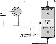
1. The emitter, which is the first letter in the NPN sequence, is connected to the negative side of the battery while the base, which is the second letter (NPN), is connected to the positive side. 2. However, since the second PN junction is required to be reverse biased for proper transistor operation, the collector must be connected to an opposite polarity voltage (positive) than that indicated by its letter designation(NPN). The voltage on the collector must also be more positive than the base, as shown below:
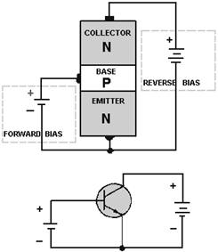
We now have a properly biased NPN transistor. Just as in the case of the PN junction diode, the N material comprising the two end sections of the NPN transistor contains a number of free electrons, while the center P section contains an excess number of holes. The action at each junction between these sections is the same as that previously described for the diode; that is, depletion regions develop and the junction barrier appears. To use the transistor as an amplifier, each of these junctions must be modified by some external bias voltage. For the transistor to function in this capacity, the first PN junction (emitter-base junction) is biased in the forward, or low-resistance, direction. At the same time the second PN junction (base-collector junction) is biased in the reverse, or high-resistance, direction. a simple way to remember how to properly bias a transistor is to observe the NPN or PNP elements that make up the transistor. The letters of these elements indicate what polarity voltage to use for correct bias. For instance, notice the NPN transistor to the right. In summary, the base of the NPN transistor must be positive with respect to the emitter, and the collector must be more positive than the base. NPN Forward-Biased Junction
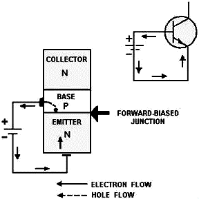
Figure 2-5 - The forward-biased junction in an NPN transistor. An important point to bring out at this time, which was not necessarily mentioned during the explanation of the diode, is the fact that the N material on one side of the forward-biased junction is more heavily doped than the P material. This results in more current being carried across the junction by the majority carrier electrons from the N material than the majority carrier holes from the P material. Therefore, conduction through the forward-biased junction, as shown in figure 2−5, is mainly by majority carrier electrons from the N material (emitter). With the emitter-to-base junction in the figure biased in the forward direction, electrons leave the negative terminal of the battery and enter the N material (emitter). Since electrons are majority current carriers in the N material, they pass easily through the emitter, cross over the junction, and combine with holes in the P material (base). For each electron that fills a hole in the P material, another electron will leave the P material (creating a new hole) and enter the positive terminal of the battery. NPN Reverse-Biased Junction
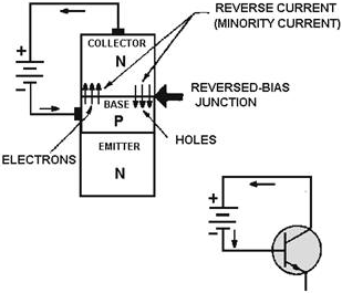
Figure 2-6 - The reverse-biased junction in an NPN transistor. The second PN junction (base-to-collector), or reverse- biased junction as it is called (fig. 2-6), blocks the majority current carriers from crossing the junction. However, there is a very small current, mentioned earlier, that does pass through this junction. This current is called minority current, or reverse current. As you recall, this current was produced by the electron-hole pairs. The minority carriers for the reverse-biased PN junction are the electrons in the P material and the holes in the N material. These minority carriers actually conduct the current for the reverse-biased junction when electrons from the P material enter the N material, and the holes from the N material enter the P material. However, the minority current electrons (as you will see later) play the most important part in the operation of the NPN transistor. At this point you may wonder why the second PN junction (base-to-collector) is not forward biased like the first PN junction (emitter-to-base). If both junctions were forward biased, the electrons would have a tendency to flow from each end section of the N P N transistor (emitter and collector) to the center P section (base). In essence, we would have two junction diodes possessing a common base, thus eliminating any amplification and defeating the purpose of the transistor. a word of caution is in order at this time. If you should mistakenly bias the second PN junction in the forward direction, the excessive current could develop enough heat to destroy the junctions, making the transistor useless. Therefore, be sure your bias voltage polarities are correct before making any electrical connections. NPN Junction Interaction
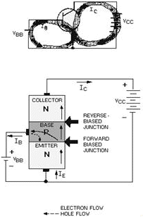
Figure 2-7 - NPN transistor operation. We are now ready to see what happens when we place the two junctions of the NPN transistor in operation at the same time. For a better understanding of just how the two junctions work together, refer to figure 2-7 during the discussion. The bias batteries in this figure have been labeled V CC for the collector voltage supply, and VBB for the base voltage supply. Also notice the base supply battery is quite small, as indicated by the number of cells in the battery, usually 1 volt or less. However, the collector supply is generally much higher than the base supply, normally around 6 volts. As you will see later, this difference in supply voltages is necessary to have current flow from the emitter to the collector. As stated earlier, the current flow in the external circuit is always due to the movement of free electrons. Therefore, electrons flow from the negative terminals of the supply batteries to the N-type emitter. This combined movement of electrons is known as emitter current (IE). Since electrons are the majority carriers in the N material, they will move through the N material emitter to the emitter-base junction. With this junction forward biased, electrons continue on into the base region. Once the electrons are in the base, which is a P-type material, they become minority carriers. Some of the electrons that move into the base recombine with available holes. For each electron that recombines, another electron moves out through the base lead as base current IB (creating a new hole for eventual combination) and returns to the base supply battery VBB. The electrons that recombine are lost as far as the collector is concerned. Therefore, to make the transistor more efficient, the base region is made very thin and lightly doped. This reduces the opportunity for an electron to recombine with a hole and be lost. Thus, most of the electrons that move into the base region come under the influence of the large collector reverse bias. This bias acts as forward bias for the minority carriers (electrons) in the base and, as such, accelerates them through the base-collector junction and on into the collector region. Since the collector is made of an N-type material, the electrons that reach the collector again become majority current carriers. Once in the collector, the electrons move easily through the N material and return to the positive terminal of the collector supply battery VCC as collector current (IC).
Posted September 10, 2021
|
||||||||||||||||||||||||||||||||||||||||||||||||||