Module 7 − Introduction to Solid−State Devices and Power Supplies
Pages i ,
1−1,
1−11,
1−21,
1−31,
1−41,
2−1,
2−11,
2−21,
2−31,
2−41,
2−51,
3−1,
3−11,
3−21,
3−31,
3−41,
3−51,
4−1 to 4−10,
4−11,
4−21,
4−31,
4−41,
4−51, Index
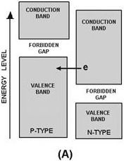
Figure 3-7A. - Tunnel diode energy diagram with 50 millivolts bias.
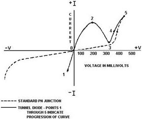
Figure 3-7B. - Tunnel diode energy diagram with 50 millivolts bias. Figure 3-8, view A, is the energy diagram of a tunnel diode in which the forward bias has been increased
to 450 millivolts. As you can see, the valence band and the conduction band no longer overlap at this point, and
tunneling can no longer occur. The portion of the curve in view B from point 2 to point 3 shows the decreasing
current that occurs as the bias is increased, and the area of overlap becomes
3-11
smaller. As the overlap between the two energy bands becomes smaller, fewer and fewer electrons can
tunnel across the junction. The portion of the curve between point 2 and point 3 in which current decreases as the
voltage increases is the negative resistance region of the tunnel diode.
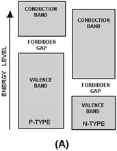
Figure 3-8A. - Tunnel diode energy diagram with 450 millivolts bias.
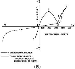
Figure 3-8B. - Tunnel diode energy diagram with 450 millivolts bias. Figure 3-9, view A, is the energy diagram of a tunnel diode in which the forward bias has been increased
even further. The energy bands no longer overlap and the diode operates in the same manner as a normal PN
junction, as shown by the portion of the curve in view (B) from point 3 to point 4.
3-12
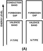
Figure 3-9A. - Tunnel diode energy diagram with 600 millivolts bias.
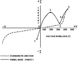
Figure 3-9B. - Tunnel diode energy diagram with 600 millivolts bias. The negative resistance region is the most important and most widely used characteristic of the tunnel
diode. a tunnel diode biased to operate in the negative resistance region can be used as either an oscillator or
an amplifier in a wide range of frequencies and applications. Very high frequency applications using the tunnel
diode are possible because the tunneling action occurs so rapidly that there is no transit time effect and
therefore no signal distortion. Tunnel diodes are also used extensively in high-speed switching circuits because
of the speed of the tunneling action. Several schematic symbols are used to indicate a tunnel diode. These
symbols are illustrated in figure 3-10 (view A, view B, view C, and view D).
3-13
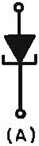
Figure 3-10A. - Tunnel diode schematic symbols.
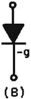
Figure 3-10B. - Tunnel diode schematic symbols.
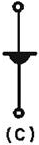
Figure 3-10C. - Tunnel diode schematic symbols.
3-14
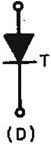
Figure 3-10D. - Tunnel diode schematic symbols. Varactor The VARACTOR, or varicap, as the schematic drawing in figure 3-11 suggests,
is a diode that behaves like a variable capacitor, with the PN junction functioning like the dielectric and plates
of a common capacitor. Understanding how the varactor operates is an important prerequisite to understanding
field-effect transistors, which will be covered later in this topic.
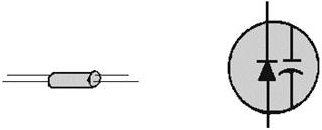
Figure 3-11. - Varactor diode. Figure 3-12 shows a PN junction. Surrounding the junction of the P and N materials is a narrow region
void of both positively and negatively charged current carriers. This area is called the depletion region.
3-15
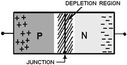
Figure 3-12. - PN junction. The size of the depletion region in a varactor diode is directly related to the bias. Forward biasing
makes the region smaller by repelling the current carriers toward the PN junction. If the applied voltage is large
enough (about .5 volt for silicon material), the negative particles will cross the junction and join with the
positive particles, as shown in figure 3-13. This forward biasing causes the depletion region to decrease,
producing a low resistance at the PN junction and a large current flow across it. This is the condition for a
forward-biased diode. On the other hand, if reverse-bias voltage is applied to the PN junction, the size of its
depletion region increases as the charged particles on both sides move away from the junction. This condition,
shown in figure 3-14, produces a high resistance between the terminals and allows little current flow (only in the
microampere range). This is the operating condition for the varactor diode, which is nothing more than a special
PN junction.
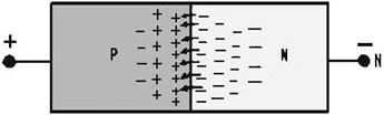
Figure 3-13. - Forward-biased PN junction.
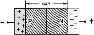
Figure 3-14. - Reverse-biased PN junction.
3-16
As the figure shows, the insulation gap formed by reverse biasing of the varactor is comparable to the
layer of dielectric material between the plates of a common capacitor. Furthermore, the formula used to calculate
capacitance

Where A = plate area K = a constant value d = distance between plates can be applied to both the varactor and the capacitor. In this case, the size of the insulation gap of
the varactor, or depletion region, is substituted for the distance between the plates of the capacitor. By varying
the reverse-bias voltage applied to the varactor, the width of the "gap" may be varied. An increase in reverse
bias increases the width of the gap (d) which reduces the capacitance (C) of the PN junction. Therefore, the
capacitance of the varactor is inversely proportional to the applied reverse bias. The ratio of varactor
capacitance to reverse-bias voltage change may be as high as 10 to 1. Figure 3-15 shows one example of the
voltage-to-capacitance ratio. View a shows that a reverse bias of 3 volts produces a capacitance of 20 picofarads
in the varactor. If the reverse bias is increased to 6 volts, as shown in view B, the depletion region widens and
capacitance drops to 5 picofarads. Each 1-volt increase in bias voltage causes a 5-picofarad decrease in the
capacitance of the varactor; the ratio of change is therefore 5 to 1. Of course any decrease in applied bias
voltage would cause a proportionate increase in capacitance, as the depletion region narrows. Notice that the
value of the capacitance is small in the picofarad range.
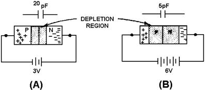
Figure 3-15. - Varactor capacitance versus bias voltage. In general, varactors are used to replace the old style variable capacitor tuning. They are used in
tuning circuits of more sophisticated communication equipment and in other circuits where variable capacitance is
required. One advantage of the varactor is that it allows a dc voltage to be used to tune a circuit for simple
remote control or automatic tuning functions. One such application of the varactor is as a variable tuning
capacitor in a receiver or transmitter tank circuit like that shown in figure 3-16.
3-17
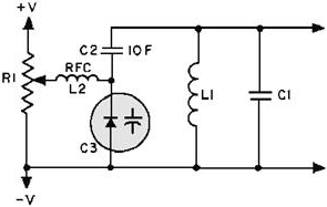
Figure 3-16. - Varactor tuned resonant circuit. Figure 3-16 shows a dc voltage felt at the wiper of potentiometer R1 which can be adjusted between +V
and -V. The dc voltage, passed through the low resistance of radio frequency choke L2, acts to reverse bias
varactor diode C3. The capacitance of C3 is in series with C2, and the equivalent capacitance of C2 and C3 is in
parallel with tank circuit L1-C1. Therefore, any variation in the dc voltage at R1 will vary both the capacitance
of C3 and the resonant frequency of the tank circuit. The radio-frequency choke provides high inductive reactance
at the tank frequency to prevent tank loading by R1. C2 acts to block dc from the tank as well as to fix the
tuning range of C3.
An ohmmeter can be used to check a varactor diode in a circuit. a high reverse-bias resistance and a low
forward-bias resistance with a 10 to 1 ratio in reverse-bias to forward-bias resistance is considered normal.
Q7. What is the main difference in construction between normal PN junction diodes and tunnel diodes?
Q8. What resistance property is found in tunnel diodes but not in normal diodes? Q9. When compared to
the ordinary diode, the tunnel diode has what type of depletion region? Q10. In the tunnel diode, the
tunneling current is at what level when the forbidden gap of the N-type material is at the same energy level as
the empty states of the P-type material? Q11. The varactor displays what useful electrical property?
Q12. When a PN junction is forward biased, what happens to the depletion region? Q13. When the
reverse bias on a varactor is increased, what happens to the effective capacitance? Silicon
Controlled Rectifier (SCR) The SILICON Controlled RECTIFIER, usually referred to as an SCR, is
one of the family of semiconductors that includes transistors and diodes. a drawing of an SCR and its schematic
representation is shown in views a and B of figure 3-17. Not all SCRs use the casing shown, but this is typical of
most of the high-power units.
3-18
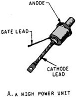
Figure 3-17A. - Silicon controlled rectifier.
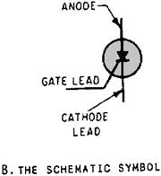
Figure 3-17B. - Silicon controlled rectifier. Although it is not the same as either a diode or a transistor, the SCR combines features of both.
Circuits using transistors or rectifier diodes may be greatly improved in some instances through the use of SCRs.
The basic purpose of the SCR is to function as a switch that can turn on or off small or large amounts of power.
It performs this function with no moving parts that wear out and no points that require replacing. There can be a
tremendous power gain in the SCR; in some units a very small triggering current is able to switch several hundred
amperes without exceeding its rated abilities. The SCR can often replace much slower and larger mechanical
switches. It even has many advantages over its more complex and larger electron tube equivalent, the thyratron.
3-19
The SCR is an extremely fast switch. It is difficult to cycle a mechanical switch several hundred
times a minute; yet, some SCRs can be switched 25,000 times a second. It takes just microseconds (millionths of a
second) to turn on or off these units. Varying the time that a switch is on as compared to the time that it is off
regulates the amount of power flowing through the switch. Since most devices can operate on pulses of power
(alternating current is a special form of alternating positive and negative pulse), the SCR can be used readily in
control applications. Motor-speed controllers, inverters, remote switching units, controlled rectifiers, circuit
overload protectors, latching relays, and computer logic circuits all use the SCR. The SCR is made up of
four layers of semiconductor material arranged PNPN. The construction is shown in view a of figure 3-18. In
function, the SCR has much in common with a diode, but the theory of operation of the SCR is best explained in
terms of transistors.
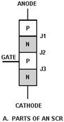
Figure 3-18A. - SCR structure. Consider the SCR as a transistor pair, one PNP and the other NPN, connected as shown in views B and C.
The anode is attached to the upper P-layer; the cathode, C, is part of the lower N-layer; and the gate terminal,
G, goes to the P-layer of the NPN triode.
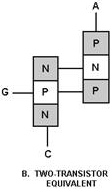
Figure 3-18B. - SCR structure. 3-20
| - |
Matter, Energy,
and Direct Current |
| - |
Alternating Current and Transformers |
| - |
Circuit Protection, Control, and Measurement |
| - |
Electrical Conductors, Wiring Techniques,
and Schematic Reading |
| - |
Generators and Motors |
| - |
Electronic Emission, Tubes, and Power Supplies |
| - |
Solid-State Devices and Power Supplies |
| - |
Amplifiers |
| - |
Wave-Generation and Wave-Shaping Circuits |
| - |
Wave Propagation, Transmission Lines, and
Antennas |
| - |
Microwave Principles |
| - |
Modulation Principles |
| - |
Introduction to Number Systems and Logic Circuits |
| - |
- Introduction to Microelectronics |
| - |
Principles of Synchros, Servos, and Gyros |
| - |
Introduction to Test Equipment |
| - |
Radio-Frequency Communications Principles |
| - |
Radar Principles |
| - |
The Technician's Handbook, Master Glossary |
| - |
Test Methods and Practices |
| - |
Introduction to Digital Computers |
| - |
Magnetic Recording |
| - |
Introduction to Fiber Optics |
| Note: Navy Electricity and Electronics Training
Series (NEETS) content is U.S. Navy property in the public domain. |
|