Crystal Diodes in Modern Electronics |
||
Diode characteristics and their applications have not changed fundamentally since this article was published in 1952. Sure, the die are smaller, power handling and frequency range has increased, package styles are greatly expanded, and the cost per unit is way down, but if you are looking for some basic diode information, you will find it here in this 4th installment of a multi-part series in Radio & Television News magazine. Don't let the vacuum tubes in schematics scare you off and think that it makes the story irrelevant for today's circuits. For purposes of illustration substitute a transistor's collector (or drain) for the tube's plate, a transistor's base (or gate) for the tube's screen grid, and a transistor's emitter (or source) for the tube's cathode. (Here is part 5) Part 4. Various applications of germanium crystal diodes as employed in present-day FM circuitry.
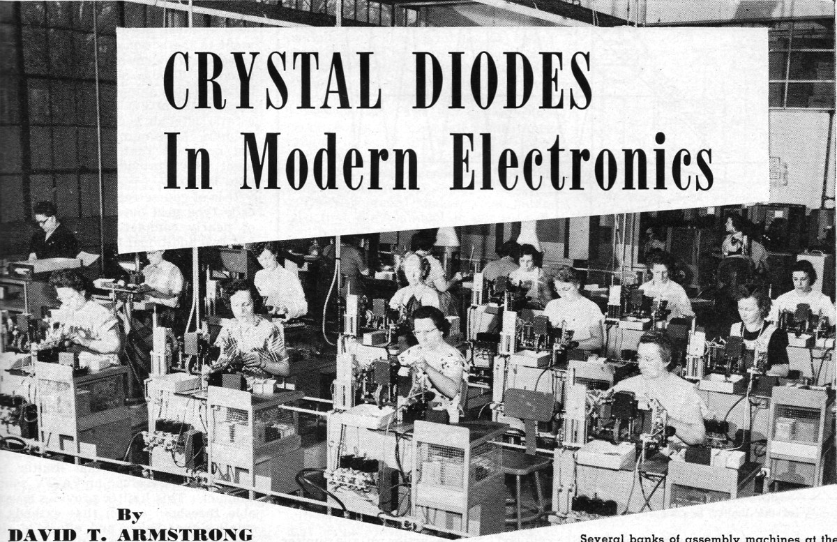
Several banks of assembly machines at the Clyde, New York plant of General Electric Company. This factory is devoted exclusively to the manufacture of germanium assemblies and other similar products. By David T. Armstrong It is assumed here that the reader has a basic understanding of FM and that he is familiar with the function of limiters, frequency discriminators, and ratio detectors. These are the important parts of an FM circuit in which crystals are beginning to play a significant role. Only those aspects of circuit considerations will be treated here which deal specifically with the application of germanium diodes to functions heretofore performed entirely by diode tubes of the 6H6 and 6AL5 types. Crystals function exceptionally well in any type of FM circuit, on i.f.'s ranging from the 4.5 mc. of the intercarrier sound system, through 10.7 and 25.75 mc., to the new 44 mc. frequency now coming into use in modern television receivers. The FM section may be a distinct entity of an FM receiver, or it may be the FM sound system in a modern television circuit. The material presented here applies equally well to any type of modern FM circuitry. Limiter Circuits One of the basic require merits of an FM system is a limiting device to eliminate amplitude variations before they reach the detector. The function of the limiter is to remove amplitude modulation and to pass on to the detector a frequency modulated signal of constant amplitude. To operate successfully, the limiter must be supplied with a sufficiently large signal voltage so that the amplitude of its output will not change with rather wide variations in signal amplitude. Noise, which causes little frequency modulation but much amplitude modulation of the received signal, is virtually wiped out in a limiter stage. Automatic volume control may be used with an FM receiver, but when a limiter is operating properly, a.v.c. is neither necessary nor desirable. The limiter is part of the final i.f. amplifier stage; its main function is to remove amplitude variations which might reach the detector and appear as distortion in the audio output. The limiter, then, is a gate which removes amplitude variations from a signal above a predetermined level and passes on a signal that is constant in amplitude. The positive and negative peaks of the FM signal will be truncated and flattened. See Fig. 1. This does not introduce distortion into the FM signal as it might in an AM signal because the modulation component or intelligence is contained in the frequency deviations of the signal and not in the amplitude variations of the signal. Frequency deviations due to modulation are not affected by limiter action.
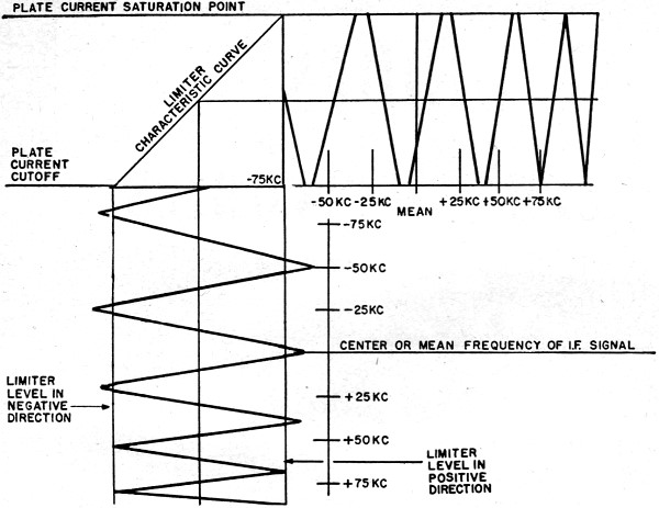
Fig. 1 - Limiter action for a strong i.f. signal. Note that the amplitude of the input wave at the highest frequency deviation components of the FM wave is above the limiter level, and that the input level of the i.f. signal over the entire range of the frequency deviations is above the limiter level. Also note that positive and negative peaks of the output FM wave are truncated. The output of the limiter is constant over the entire range of the frequency deviation.
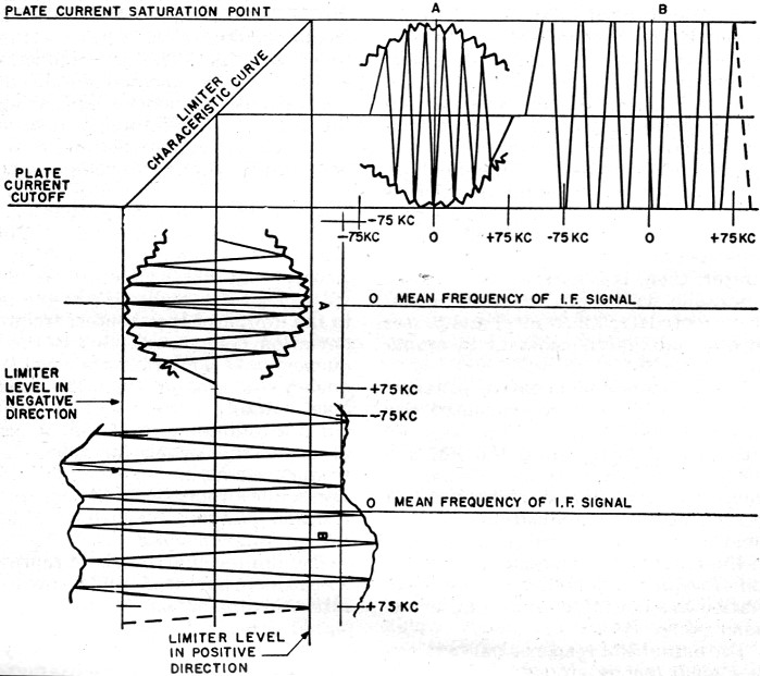
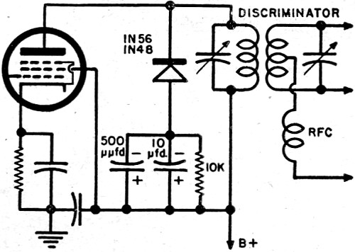
Fig. 2 - Effect of limiter action on varying limiter input signals. (A) Noise voltage reproduced in the output of limiter. (B) Noise is removed by limiter action, wave is truncated. Note that when the input level of the i.f. signal over the entire range of frequency deviation is above the limiter threshold, as in (B), no noise voltage is reproduced in the output of the limiter but when the input level of the i.f. signal is below the threshold of limiter action, the limiter cannot function and the noise will be reproduced as shown in (A). The actual FM response curve is nei-ther ideal nor flat topped. Hence the various frequencies making up the total frequency deviation will not have the same relative amplitude at the input to the limiter. The center frequency and the frequencies close to it will have greater amplitude than those considerably removed from the center frequency due to the action of the i.f. tuned circuits. This is demonstrated in Fig. 2. The unequal amplitude of the various frequencies appearing at the input to the limiter would cause severe distortion if something were not done in the receiver to compensate for it. A limiter is sometimes regarded as a device for removing all noise. This is not so. A limiter will function efficiently (but not perfectly) when the voltage level (amplitude) at the input to the limiter of the greatest frequency deviation component (this is the frequency ± 75 kc. from the mean frequency) is greater than the limiting level. Limiter output will be constant when a total band of 150 kc. is passed at a constant level, for then all the frequencies making up the total deviation will be reproduced in their proper relation, and without distortion due to AM or random noise. The limiter characteristic represented by the graph at A in Fig. 2 will permit AM distortion because the i.f. signal is below the limiter level. Note that the limiter level is gauged by the characteristic curve of the voltage-frequency graph. The signal at B will permit no distortion because the lowest signal input level is above the limiter level. Hence all AM components and/or random noise are "hedge clipped" by the action of the limiter. Diode Dynamic Limiter Any residual amplitude modulation and noise riding the FM wave should be suppressed. The limiter component desired must be an effective supplement to the action of the FM detector to reduce random noise and AM interference. This is necessary because a balanced discriminator completely suppresses AM at but one frequency, and a ratio detector is critical to align and balance. Maximum AM rejection may not occur at that alignment adjustment which provides the most desirable linearity. It is of course recognized that a cascade type grid bias limiter is capable of nearly complete AM suppression; but two additional tubes are necessary and this type of circuit is relatively expensive. A comparative set of curves for one diode, two diodes, and a cascade limiter is shown in Fig. 3. The single and double diode curves are variable threshold devices that show AM reduction factors ranging from 6 to 10 db better than the cascade limiter for signal levels below the threshold of the cascade type limiter. Fig. 4 shows a dynamic limiter circuit employing a type 1N48 or 1N56 as the germanium crystal diode. This is a simple and highly effective type of amplitude modulation limiter for both an FM receiver and a TV sound channel. This limiter provides a variable threshold action that extends to small signal levels and effects a significant degree of quieting on weak signals as well as for interchannel background noise. Any signal of such peak amplitude as to be above the threshold level will have its residual amplitude variations suppressed by this limiter. The ideal limit of suppression may be more nearly approached by a germanium crystal than by a vacuum tube, because the crystal exhibits so much greater conductance than a tube. In addition to high conductance, the crystal diode exhibits extremely low capacitance. This variable threshold limiter device uses a resistance-capacitance network with a time constant long compared to the lowest expected amplitude modulation frequency, and the limiter adjusts itself automatically to the varying average signal amplitude. A time constant of 0.1 second is sufficient to insure rejection of AM components down to 10 cycles. For a given frequency there is a loss caused by the insertion of a diode in a transmission system. It is the ratio, expressed in decibels, of, the power delivered before the insertion to the power delivered after the insertion; this is commonly referred to as "insertion loss." Since for any given signal level the insertion loss of the limiter becomes greater as the resistance is reduced, the resistance value is governed by the allowable limiter insertion loss and the desired degree of small signal AM rejection. 10,000 ohms is a reasonable compromise among all the factors which obtain. To achieve a time constant of 0.1 second the value of the electrolytic type condenser then becomes 10 μfd.; for a 20,000 ohm resistor it would be 5 μfd. The small 500 μμfd. mica condenser bypasses the high frequency i.f. components.
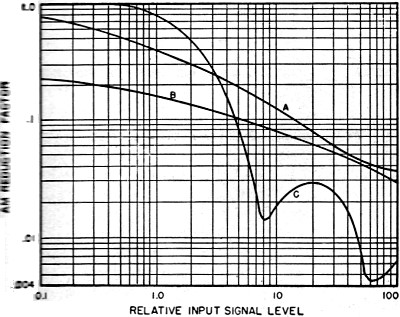
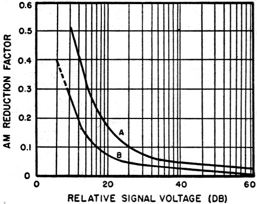
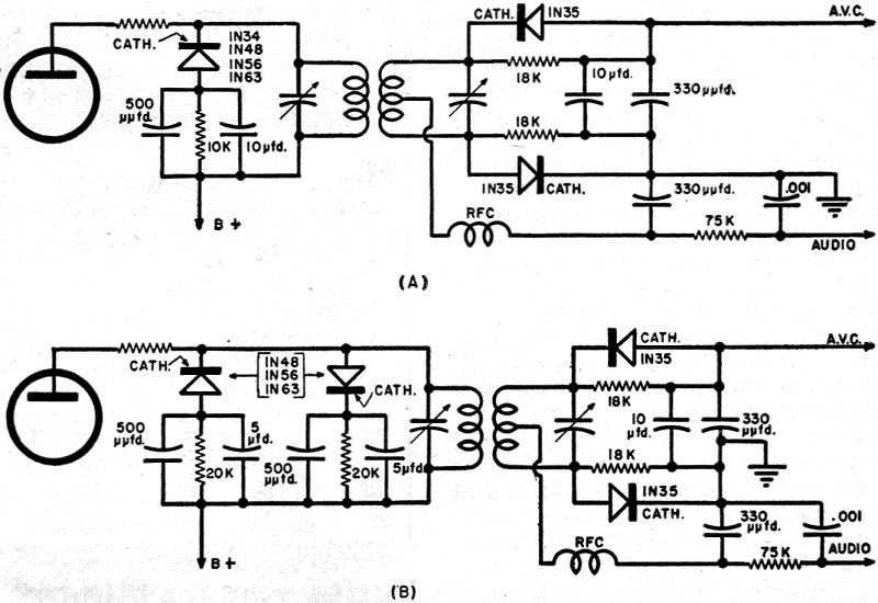
Fig. 3 - Comparison of single and double diodes with cascade type grid bias limiter. (A) Single diode dynamic limiter (IN56), (B) Double diode dynamic limiter (2-IN56's) end (C) Cascade limiter using 2-6SJ7 tubes.
Fig. 4 - Single diode dynamic limiter. The values of the 10,000 ohm resistor and the 10 μfd. condenser may be chosen to suit the signal frequency and degree of clipping desired. Values of the resistor may range from 5000 to 50,000 ohms. Condenser values will depend on the time constant desired. The time constant of this circuit is approximately 0.1 second. Where high impedances are desirable G-E types 1N52 or 1N63 or Sylvania type 1N54 may be employed. With this type variable threshold limiter AM reduction varies smoothly with signal level, AM noise decreasing as the signal level increases, and approaching zero as the signal voltage is increased by virtue of improvement in crystal efficiency at high signal voltages. The biased high conductance diode 1N48 or 1N56 is shunted across the tuned circuit which is the primary of the detector input transformer, either limiter-discriminator or ratio detector type. Whenever the "Q" of the tuned circuit exceeds 25, the damping provided by the diode is effectively integrated over the i.f. cycle. Voltage regulation is predominantly in the tuned circuit, and the diode helps maintain essentially constant voltage across the circuit. This type dynamic limiter is not critical with respect to characteristics of the particular crystal employed; virtually any germanium diode will perform well in this circuit. This is a worthwhile consideration in connection with replacement of one unit by another. Further, the back resistance of the crystal also serves to augment the action of the limiter. Finally, a receiver using a dynamic limiter would require only 1/2 to 1/3 the input signal voltage at the antenna to produce a given amount of quieting. Of course this limiter is not capable of as great AM suppression as the cascade grid bias type limiter. However, the variable threshold action tends to extend the range of operation to low signal levels. Thus the use of such a dynamic limiter in simplified FM receivers is attractive because of the significant quieting on weak signals, even with but slight over-all gain. In the absence of a signal some squelch action occurs as a result of partial limiting on receiver background noise. In a TV receiver with intercarrier sound this type dynamic limiter helps to reduce the audio buzz which sometimes accompanies excessive modulation depth of the picture carrier. The double diode dynamic limiter circuit shown in Fig. 5, used in conjunction with an FM detector, helps suppress residual AM in frequency modulation type receivers or sound circuits of TV receivers. A high conductance diode like the 1N56 provides exceptionally effective limiter action, particularly at signal levels as low as 5 volts or less. The low dynamic impedance and the low diode capacitance produce a minimum of reactive loading across the source and minimize any loss traceable to limiter insertion at low signal levels. The two biased diodes are so polarized that they conduct in opposite directions. The net improvement in AM reduction factor (ratio of the percentage modulation of output signal to input signal) is so exceptional that it is shown graphically in Fig. 6. Many television receivers use a limiter stage ahead of the discriminator, even when a ratio detector is used as the detector. The function of the limiter is to clip off any amplitude variations of the sound i.f. signal that may be caused by noise or non-uniform i.f. amplification over the frequency band. Wherever the normal amplification of the grid biased limiter is not necessary, a biased diode may be used more economically. The basic limiter circuit in Fig. 4 illustrates this effectively. The diode with a bias voltage equal to the normal signal level is placed across a tuned circuit. The diode will conduct only on peaks that exceed the normal signal level; hence noise peaks will be automatically shorted out. Harmonic distortion as a result of such clipping action may be minimized by using two diodes to clip both the positive and negative peaks, as in Fig. 5. This is, in effect, a full-wave limiter. The bias is usually obtained from an RC circuit so designed and with such a time constant configuration that it automatically adjusts itself to the signal level. This use of crystal diodes is one of the most inexpensive means of securing desirable limiter action. These germanium diodes are quite likely to be used widely in discriminator circuits. They may be wired directly to the transformer and mounted in the shielded can to facilitate elimination of contact potential feedback and filament hum problems. Discriminator Circuits
Fig. 5 - Double diode dynamic limiter circuit.
Fig. 6 - Comparison of AM reduction factor for single and double diode dynamic limiter.
Fig. 7 - Characteristic curve for a discriminator. Note that output voltage of unit is greater for a high input voltage level as shown in curve B as compared with lower input level for curve A. Also the quality of response depends on linearity of curve , from -75 kc. to +75 kc. deviation from center frequency of i.f. response. This graph demonstrates that output of the discriminator may vary with changes in signal level (which is AM variation since curves for B and A show characteristics for different signal levels).
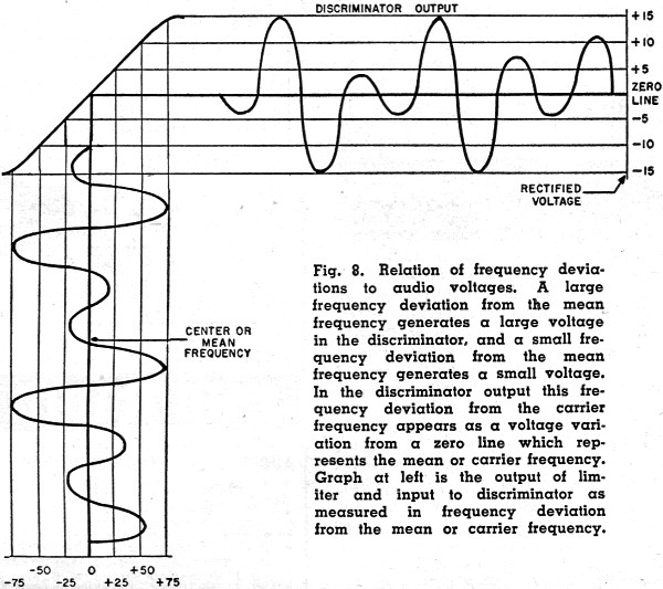
Fig. 8 - Relation of frequency deviations to audio voltages. A large frequency deviation from the mean frequency generates a large voltage in the discriminator, and a small frequency deviation from the mean frequency generates a small voltage. In the discriminator output this frequency deviation from the carrier frequency appears as a voltage variation
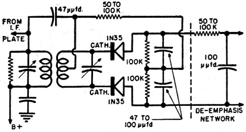
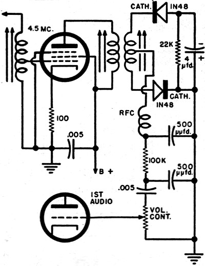
Fig. 9 - FM discriminator circuit using germanium diode crystals. The IN35 duo-diode, consisting of carefully matched crystals, is highly satisfactory for this circuit. IN35's are matched in forward resistance only and since this resistance is small compared to 100,000 ohm load, balance is unimportant. The necessary balance is in back resistance which is not very much greater than 100,000 ohms. This is one reason why shunting resistors are suggested in Fig. 10. Use of shunting resistors will permit the use of less expensive IN34 type crystals. The 100,000 ohm resistors and 47 μμfd. condensers should be low tolerance matched components for ideal balance of two parts of circuit. The de-emphasis circuit network is shown only to indicate parts values.
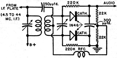
Fig. 10 - Frequency discriminator circuit. This circuit performs as well as that shown in Fig. 9 but eliminates the need for using matched diodes by using 220,000 ohm resistors in parallel with IN48 type diode crystals. Circuit is thus balanced regardless of back resistance of diodes. Other component values are typical of those found in a discriminator circuit. One of the basic requirements of an FM system is that the detector be a device for converting frequency changes into amplitude variations which may then be amplified as audio signals. In the widely used Foster-Seeley discriminator the signal frequency varies back and forth across the resonant frequency of the discriminator and an a.c. voltage of the same frequency as the original modulation is developed and passed on to the audio amplifier. The discriminator in an FM circuit corresponds to the detector in an AM circuit in that both demodulate the intelligence from the carrier wave. The process is different, but the net result is substantially the same. The voltage versus frequency characteristic for an FM discriminator is shown in Fig. 7. The total voltage output of a discriminator varies in a positive and negative direction depending upon the deviation of the i.f. signal above or below the mean frequency. The greater the frequency deviation the greater the voltage developed. The output voltage is the algebraic sum of the voltages developed across the load resistors of the two diodes. It should be apparent from the curve shown that if the straight portion of the discriminator voltage frequency curve covers a wider range of frequencies than those generated by the transmitter, the audio output will be reduced from the maximum value of which the receiver is capable. This must be so because at its "center" frequency the discriminator produces zero output voltage. On either side of this center frequency there is developed a voltage of a polarity and magnitude that depends upon the direction and amount of frequency shift from the center frequency. Therefore, the voltage output of a discriminator varies in precisely the same fashion as the audio voltage which modulates the carrier. The greater the voltage developed across the diode load the louder the sound coming from the speaker. When there is no modulation on the FM carrier there is no deviation of frequency and consequently no audio voltage is developed; hence, no sound comes from the speaker. But there is an important point to be made in connection with a discriminator detector. The output voltage of a discriminator may vary directly with change in input voltage. The curves marked A and B in Fig. 7 indicate this fact. This is why a limiter circuit is important. It holds the input level at constant amplitude and does not permit the discriminator to receive signals that are amplitude modulated. The reason why amplitude modulated signals might appear at the discriminator in an FM circuit was discussed before in connection with the limiter, where it was shown that since the response curve is not perfectly flat topped, there is some variation in the signal level which is, in effect, amplitude modulation of an FM signal wave. The method of conversion of frequency changes into audio voltage is graphically illustrated as a function of the linear portion of the discriminator characteristic, shown in Fig. 8. The circuit of Fig. 9 is a simple discriminator detector circuit. The better the matching of the diodes the better the performance of this type circuit; but note the remarks in the caption. This circuit will operate over the entire range of commonly encountered i.f. frequencies from the 4.5 mc. used with intercarrier sound to the 44 mc. i.f. The crystals and associated resistors and condensers may be mounted under the chassis or they may be enclosed in a small shield can. In some instances, by careful layout and design, it is possible to include the diode crystals, resistors, and condensers in the FM discriminator shield can. Such location is important in preventing feedback. This makes a most compact assembly although it does present servicing difficulties. The circuit shown in Fig. 10 is desirable from the standpoint that crystal matching is not necessary. The 220,000 ohm resistors in parallel with standard stock type 1N48 diodes keep the circuit balanced irrespective of the back resistance of the crystals. The other circuit values are typical of those found in a discriminator circuit. The reverse resistance of a crystal diode is subject to minor variations with changes in ambient temperature, humidity, and impressed voltage. While in general applications the small changes in back resistance are of little consequence they are significant in an FM detector because demodulation depends upon close balance between the two parts of the circuit. The better the balance the higher the degree of linearity and the greater the AM suppression for the discriminator. from a zero line which represents the mean or carrier frequency. Graph at left is the output of limiter and input to discriminator as measured in frequency deviation from the mean or carrier frequency. The sound circuit of a television receiver is the same as that found in a typical FM receiver. Detection of the i.f. signal is accomplished by a discriminator or a ratio detector circuit. Both types of circuit require two diodes and balanced conditions for optimum operation. Germanium diodes have been successfully substituted for vacuum tube diodes in a discriminator circuit; probably the most widely used discriminator is the Foster-Seeley type. The chief circuit difference for crystals as compared to the vacuum tube is the use of shunting resistors with the crystals to maintain fairly uniform balance between both halves of the circuit with respect to the back resistance characteristics. Ratio Detector Circuits A discriminator detector requires one and preferably two limiter stages because of discriminator sensitivity to amplitude as well as to frequency variations. For effective limiting there must be good amplification of the i.f. signal before it reaches the limiter in order that all signals have a level sufficiently high to operate the limiter at saturation. Since a ratio detector does not respond appreciably to amplitude variations it is, from that point of view, superior to a discriminator type detector. The chief advantage of a ratio detector is that for a weak carrier, on modulation, the voltage ratio is the same as for a strong carrier, on modulation; therefore, the ratio detector is not responsive to carrier changes, and hence relatively insensitive to either sudden or dynamic changes in amplitude of the applied signal. Because a ratio detector is responsive to slow changes in carrier, a.v.c. may be desirable. The audio output deriving from frequency modulation of the applied signal results from the change in the ratio of the two diode voltages which makes the circuit responsive mainly to variations in signal frequency and not to dynamic changes in signal amplitude. With a ratio detector circuit, balance between the halves of the system is more critical than for a discriminator type circuit. The ratio detector provides AM suppression as well as FM detection and its operation depends, to a great extent, on the balance between the halves of the system. The back resistance of crystals is not uniform and changes with temperature and voltage level; the situation is complicated by the fact that the changes are not likely to be the same in both diodes, nor to occur at the same time. It is therefore more difficult to design a ratio detector system using germanium diodes, but it is not impossible. Variations of the ratio detector circuit have been designed to minimize any detrimental and undesirable effects of the back resistance characteristics of the crystals. Although these circuits do not achieve all the good inherent in the ratio detector system, they do approach the operating quality of conventional vacuum tube circuits. The ratio detector has excellent inherent noise and AM reduction characteristics, and the conventional circuit using a 6AL5 is economical. But it is not possible to simplify the conventional ratio detector circuit just by inserting germanium diode crystals as substitutions for the separate halves of the 6AL5. The dynamic characteristics of a crystal are somewhat different from those of a vacuum tube diode. However, experimental work with the ratio detector circuit has facilitated the development of a crystal diode ratio detector circuit that provides performance data approximately equivalent to that obtainable from a vacuum tube. The crystal diode circuit has excellent physical advantages over the vacuum tube diode with respect to savings in weight, power, and space, making possible the development of battery-operated, portable-type FM receivers. The ratio detector circuit depends critically upon close balance between the two individual parts of the circuit in order to obtain a high degree of linearity and to provide the amount of AM suppression desirable in an FM receiver. The modified form of ratio detector circuit here presented will yield results comparable to those achievable by a vacuum tube circuit, assuming that both units are properly designed and equally well constructed. The combined load circuit shown in Fig. 11, has a time constant long with respect to the period of any AM components present and causes the sum of the diode output voltages to remain constant as far as AM components are concerned. Since the sum of the diode voltages is thus fixed by the long time constant load circuit, the ratio detector is not responsive to the dynamic changes in the amplitude of the signal. The audio output due to frequency modulation of the applied signal results from a change in the magnitude of the two diode voltages, the net effect of which is to make the circuit responsive only to variations in signal frequency and not to dynamic changes in signal amplitude. Thus AM components due to noise and multipath transmission effects are largely suppressed in the ratio detector.
Fig. 11 - Crystal diode shunt ratio detector.
Fig. 12 - Effect of single crystal diode dynamic limiter on AM reduction factor for shunt crystal diode ratio detector. (A) Crystal diode ratio detector only. (B) Crystal diode ratio detector and dynamic limiter.
Fig. 13 - The effect of a single diode dynamic limiter on the AM reduction factor over entire band of operating frequencies.
Fig. 14- Dynamic limiter and ratio detector with (A) single and (B) double diodes.
Fig. 15 - One manufacturer's commercial adaptation of a ratio detector circuit. To obtain maximum suppression of amplitude variations in the output of the ratio detector, it is essential that the two halves of the circuit be balanced and remain so throughout the entire dynamic range of the input signal. This requires close tolerances in the resistance and capacitance values and careful design of the input transformer primary, secondary, and tertiary windings, as well as close matching of the diode characteristics. The close matching of the diode characteristics is most critical; for this reason it is generally necessary to supplement the ratio detector with some means of AM reduction before the ratio detector stage. In this one respect crystals have some superiority over vacuum tube diodes. Additional details on this point will be given later. Many attempts to substitute crystal diodes for vacuum tubes in the conventional ratio detector circuit have been unsuccessful, in that little or no AM reduction was obtained, and the circuit itself proved to be unstable both with respect to symmetry of detector characteristic and permanency of alignment. However, with suitable modification of the basic circuit arrangement the undesirable effects of the variations in the back resistance of the crystal can be largely eliminated, and a germanium diode ratio detector exhibiting the characteristics of the vacuum tube diode circuit can be designed. Modifications from the conventional type ratio detector circuit are relatively minor, as can be gathered from a consideration of the modified shunt ratio detector circuit shown in Fig. 11. The load resistors for the crystals are shunt rather than series connected. Electronically, the shunt circuit is equivalent to the series circuit in that, for given values of load resistance and signal voltage, the rectification efficiency is essentially the same for both. Shunt connection of the crystal diodes makes possible the use of resistances in parallel with the crystals, each of which is of much lower value than the back resistance of the crystal across which it is connected; these resistances have the effect of swamping out the crystal back resistances. This detector circuit is relatively insensitive to changes in crystal back resistance and tends to reduce static and dynamic imbalance between the halves of the circuit. By virtue of their high conductance, crystals tend to provide somewhat improved circuit efficiency over vacuum tube diodes. Low shunting resistors, however, reduce efficiency as compared to vacuum tubes. Diode balance or AM suppression can only be obtained at the expense of output. There are numerous advantages to be gained by using crystal diodes to replace the vacuum tubes in this type of circuit: 1. Compactness - The entire assembly can be built into the same shield can as a plug-in device if one is willing to use the Vector socket technique. The associated condensers and resistors, in addition to the two germanium diodes, occupy so little space that there is plenty of room to make a complete package unit of the entire ratio detector circuit. 2. Filament Elimination - The elimination of heater requirements materially reduces hum difficulties, particularly with series heater circuits, where the potential difference between cathode and heater of a detector tube may be quite large. 3. Parts Elimination - This makes for economy in the number of component parts, such as the socket and a smaller size filament transformer, which result in a substantial saving of space and reduction of weight. 4. Imbalance Elimination - There is complete elimination of imbalance resulting from contact potential effects in diode elements. Contact potential may upset static balance between the halves of the circuit. In FM detector circuits that are properly balanced maximum AM suppression occurs at that frequency corresponding to the crossover of the detector characteristic. A crystal circuit is somewhat more susceptible to residual amplitude modulation than a 6AL5 duo-diode circuit. The load resistance in a crystal type ratio detector circuit has some effect upon circuit sensitivity as well as upon AM reduction. Sensitivity as used here indicates the ratio of the d.c. voltage across the holding condenser to the r.f. voltage across the secondary of the input transformer. On the basis of experimental curves showing circuit performance with load resistances varying from 5000 to 50,000 ohms, it has been found that the circuit is most stable when the load resistance is kept small with respect to the back resistance of the crystals. Values from 15,000 to 20,000 ohms are a nice compromise among the variety of factors which obtain. In some respects a crystal circuit is superior to a vacuum tube circuit for AM suppression, but for an off-tune signal, background noise is quite likely to be greater. On the other hand, a crystal circuit is simpler to align than a vacuum tube circuit, by virtue of elimination of contact potential imbalance effects. A ratio detector circuit may be adjusted for virtually any pair of crystals, but the AM reduction will vary from pair to pair, because of the degree of variability in the dynamic forward characteristics. With random selection of crystals an AM reduction factor of about 0.025 is possible, while with careful selection of crystals matched for similar forward dynamic characteristics the AM reduction factor is better than 0.010. Whenever it is desirable to achieve a degree of AM suppression comparable to that achieved by a vacuum tube grid bias limiter, a circuit involving a crystal diode dynamic limiter just before the ratio detector stage is indicated. In addition to providing a substantial degree of AM suppression in itself a dynamic limiter tends to minimize the necessity for AM suppression by the ratio detector. In such a combination germanium diode circuit crystal selection may be eliminated in the ratio detector stage. This is because a dynamic limiter extends AM suppression to lower input signal levels and over a wider frequency deviation range from the mean signal frequency. Fig. 12 and Fig. 13 show the AM reduction factor as a function of signal level both with and without the dynamic limiter. In summary, then, a crystal diode shunt type ratio detector combined with a crystal diode dynamic limiter will provide an audio output comparable to that obtainable with the conventional duo-diode tube ratio detector of the 6AL5 type. A suggested circuit is shown in Fig. 14. Fig. 15 shows a commercial application of the 1N48 to a good ratio detector circuit. (To be continued)
Posted November 5, 2019 |
||