VDRs and Thermistors
|
|
Pop Quiz: What is the contemporary name we have given to the voltage dependent resistor (VDR)?* Although VDRs are nowadays used most familiarly for overvoltage protection due to spikes on a power or signal line, they used to be functional parts of television display and power supply circuits. Sylvania was a prime manufacturer of VDRs, and field effect transistors - both junction (JFET), and enhancement mode and depletion mode insulated-gate (IGFET, aka MOSFET). The company used of all these devices back in the day as part of their effort to modernize televisions and radio by abandoning vacuum tubes wherever possible. Thermistors, silicon-controlled rectifiers (SCRs), and varactor diodes are also discussed in this 1969 vintage Radio−Electronics magazine article. *Answer: A varistor. VDR's and Thermistors
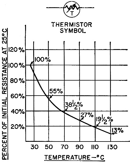
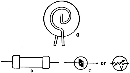
Fig. 3 - Thermistor curve. Resistance drops as temperature rises. By Sylvania Technical Staff Take a look at all the newest semiconductor devices. There are VDR's, thermistors, FET's, VVC's and more Every so often you'll have to test voltage dependent resistors (VDR's) and thermistors and then decide whether or not they should be replaced. First let's take a look at the VDR. Physically, the VDR appears as in Fig. 1-a and Fig. 1-b. Don't be fooled by the appearance of the unit in Fig. 1-b. It may look like a precision resistor but it isn't. The electronic symbols for the VDR are in Fig. 1-c. VDR's are used to present a high impedance to small applied voltage and as the voltage increases the VDR's resistance decreases and allows more and more current to flow. The VDR is used to cut pulse-peak variations by providing in a high resistance when the voltage is low, and a low resistance when the voltage is high. In the vertical circuit of a TV set it is used to provide a low resistance to the large vertical pulse during trace time, and during retrace its increased resistance allows the retrace voltage to maintain its full amplitude for fast retrace. The VDR in the video supply provides a form of regulation and filtering action in a voltage divider network.
Fig. 1- a and b - Drawings of two types of VDR's used in TV and other circuits. Two electronic symbols are shown at c.
Fig. 2 - VDR test setup. Rating is ratio of change in applied voltages required for a current change of 10.
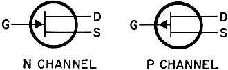
Fig. 4 - Symbols for junction-type FET's. N-channel and p-channel types. Automatic degaussing circuits in color sets use a VDR in conjunction with a thermistor to allow heavy current to flow through the degaussing coils. As soon as the temperature of the thermistor rises, the voltage across the VDR falls, its resistance increases, and current flow through the coils is effectively stopped. Most VDR's will carry 10 times more current when the voltage applied is increased one to two times over a specified range. An ohmmeter reading will tell you very little about a VDR since VDR's have such wide variation in resistance. Out-of-circuit readings will be in the megohm range. If the unit has failed it will probably fail in the open mode. Often, the easiest way to verify operation is to substitute a new VDR in place of one whose operation is questionable. Factory tests for a VDR call for a variable DC supply near the VDR voltage rating. One milliamp of current is made to flow and a voltage reading taken. When the voltage is increased until 10 milliamperes flow, the two voltages are from 1.5 to 2, as shown in Fig. 2. The rating ratio provides the change in voltage (ΔE) required to produce a change in current magnitude of 10. Most thermistors used in TV chassis have a negative temperature coefficient (NTC). Their characteristics are used where less resistance is required as a circuit comes up to temperature. (Fig. 3) One common application is to use a thermistor in series with tube heaters to protect them during heater warm-up. They are also used in the vertical output transistor amplifier to maintain constant vertical sweep voltages over the temperature range of the set. Color TV's use a thermistor to develop a voltage while still cold to divert AC to the degaussing coil circuit. A typical thermistor value when cold is 120 ohms and when hot about 20 ohms. Two ohmmeter measurements are needed to check a thermistor - the hot and the cold resistance readings. If these readings fall in the expected range the part is usually considered good. Some thermistors have hot and cold values well into the megohm range. When they fail, most thermistors increase in resistance. In a TV set this can cause slow warm-up of series-string tubes, changes in vertical height with temperature or continuous degaussing in a color set. The Field-Effect Transistor Appearing in new electronic circuitry is a new transistor type - the field-effect transistor or FET (see Fig. 4). Advantages include a high-impedance input, high-frequency response and low noise level. There is excellent input-output isolation, which is a common shortcoming of most transistors. There are two basic types: junction FET's and insulated-gate FET's.
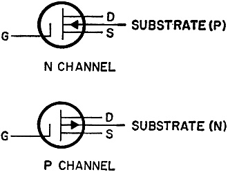
Fig. 5 - With its inherent high input impedance, the junction field-effect transistor makes an ideal RF or i.f. amplifier. A large current between drain and source can be controlled by a small voltage on the gate. When an RF voltage of a different frequency is fed to source, the FET makes a good heterodyne mixer. The basic operation of the junction FET (JFET) can be described as an electrostatic field control of current flowing through a semiconductor (see Fig. 5). The input signal provides a controlling field to the gate terminal to regulate the flow of electrons from drain to source. If the gate bias is reversed with respect to the drain source, current is reduced. If gate bias is of forward polarity, drain-source current increases. The gate bias thus varies the depletion region, reducing the channel conduction size and increasing the resistance of the channel to current flow. With a small gate voltage we can control a large source-drain current, so we have the ingredients of an amplifier. In Fig. 5 a high-impedance transformer secondary applies a small RF signal to a JFET. As shown, an oscillator signal is injected at the current-source terminal to use the stage as a superheterodyne rf-oscillator mixer. The gate terminal must never be completely forward-biased or the source-drain current will flow into the gate circuit. Insulated Gate FET This type FET has the gate junction insulated from the current-drain material by glass. This prevents drain current from flowing into the gate circuit as it did in the JFET. The principle of operation is the same as the JFET except that a higher input impedance is obtained and the DC polarity of the input signal may vary. To set up a DC operating condition, a positive polarity is applied to the drain terminal (Fig. 6). The substrate is connected to the source, and both are at ground potential so the channel electrons are attracted to the positive drain and a DC source-drain current is obtained.
Fig. 6 - Electronic symbols for the IGFET or insulated-gate FET. This type has a higher input impedance than the JFET and does not load down a signal source. Silicon Controlled Rectifiers The Silicon Controlled Rectifier (SCR) is similar to the vacuum-tube thyratron. When a voltage is placed across the anode and cathode a trigger voltage applied to the gate causes the semiconductor layers to suddenly decrease in resistance and heavy current can flow. This continues even after the gate trigger voltage is removed and as long as the cathode-anode voltage remains. A typical SCR application is as a switch to turn on a stereo indicator lamp in an FM set. In this circuit the 19-KHz subcarrier signal, which is present only during stereo reception, is used to turn on the SCR so that the 6.3 volts AC can operate the lamp. When stereo reception stops, the trigger voltage is removed and the anode-to-cathode current is shut off after the first pass of the AC voltage through zero. Varactor Diodes A varactor or variable-reactance diode is a pn junction semiconductor device in which the junction capacitance varies in relation to the junction voltage. When biased in the reverse direction, a varactor diode can be represented by a voltage-sensitive capacitance in series with a resistance. This nonlinear capacitance and low series resistance permit the device to perform frequency-multiplication, oscillation and switching functions. It is the result of a very high impurity concentration outside the depletion-layer region and a relatively low concentration at the junction. Very low noise levels are possible in circuits using varactor diodes because the main current across the junction is reactive and random-noise components are absent.
Fig. 7 - In this FM afc circuit, the capacitance of the back-biased varactor is across the oscillator tank. Mistuning or drift causes the FM detector to develop a negative correction voltage on the varactor anode. This changes the effective oscillator capacitance in the direction that restores the oscillator to the correct operating frequency.
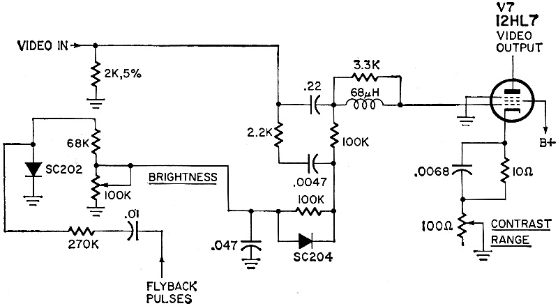
Fig. 8 - Sylvania uses diodes for DC restoration and automatic brightness control in some sets.
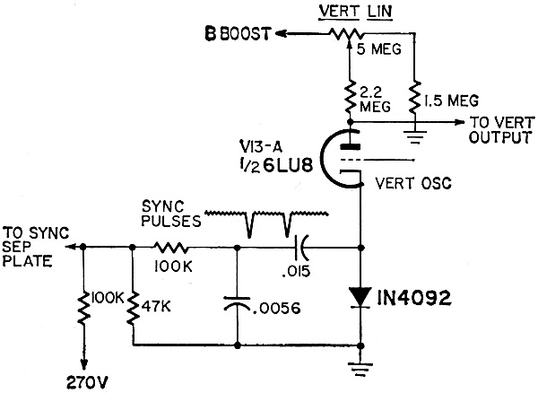
Fig. 9 - Diode in cathode circuit insures that the vertical oscillator is triggered only by the negative-going part of the sync pulse. A practical application of the varactor diode is shown in Fig. 7. The circuit permits automatic frequency control by applying an afc voltage to the cathode of the varactor diode. A fixed bias voltage is maintained on diode SC2 by resistors R38 and R40. The diode remains in a reverse-biased condition while afc voltage variations cause slight capacitance changes, maintaining a constant oscillator frequency. Clamping and Rectifying Diodes Rectifying diodes are often used as polarity switches, rectifiers and overload limiting devices. One application is as a source of DC restoration in a TV set and bias for brightness control (see Fig. 8). In this circuit SC202 rectifies a flyback pulse so that positive pulses forward-bias the diode and pull electrons up from ground. This negative charge is drained off to ground through the Brightness control. Depending on the control setting, the adjusted bias is applied to the grid of the video output stage and sets its conduction level. This establishes video plate voltages and in turn the CRT cathode bias. In series with the voltage developed by the brightness circuit is another voltage developed by rectified flyback pulses and video signal. The flyback pulse provides positive-going pulses to turn on SC204 and remove electrons from the video output grid. This is done at a level determined by the flyback pulse amplitude. When a negative polarity video signal is present, the average DC bias on the grid of V7 varies to match and the corresponding conduction change and adjusts CRT cathode bias. The CRT bias is therefore dependent upon the average video signal level. A receiver may use a clamping diode circuit to reduce the gain of an i.f. section when very strong signals are received. Normally the diode is reverse-biased until a large signal causes the diode to conduct. When the diode conducts, it loads the transformer and gain drops considerably. To troubleshoot this circuit, make sure the diode is reverse-biased under no-signal conditions. The anode of the overload diode should be negative with respect to the cathode by a volt or more with no signal. A shorted diode causes a severe gain reduction under any signal condition. An open diode results in distortion when very strong signals are received. Another application of the clamping diode is in a vertical oscillator circuit (see Fig. 9). This is a multivibrator type circuit with vertical triggering applied at the cathode of the vertical oscillator and across a diode. The diode is forward-biased to allow the tube to conduct normally. When sync pulses are applied to the diode, negative-going pulses bias the cathode and serve to trigger the tube out of the cutoff portion of its cycle. Positive-going pulses are grounded by virtue of forward-biasing the clamping diode. The diode will keep the cathode potential of V13-a from ever going positive, but will allow negative excursions resulting from sync pulses.
Posted September 18, 2023 |
|