The Tunnel Diode Story
|
|
Tunnel diodes were first developed by Dr. Leo Esaki in 1958, just two years before this article appeared in Radio-Electronics magazine. In fact, it was sometimes referred to as an Esaki diode. Dr. Esaki made a significant discovery related to quantum mechanical tunneling, which led to the development of the tunnel diode; it earned him the Nobel Prize in Physics in 1973. Quantum mechanical tunneling is a phenomenon in quantum mechanics where a particle, such as an electron, can pass through a potential barrier even when it does not have sufficient energy to surmount the barrier. This effect arises due to the wave-particle duality of quantum mechanics, which allows particles to exhibit wave-like behavior. This led to the development of the tunnel diode, a semiconductor device that takes advantage of electron tunneling. The tunnel diode is constructed with a heavily doped p-n junction, where the doping levels are carefully selected to enable the tunneling effect. The device's unique characteristic is its negative resistance region, where the current decreases as the voltage increases within a specific voltage range. The Tunnel Diode Story
The tunnel diode reported in 1958 by Japanese scientist Dr. Leo Esaki, is an entirely new semi conductor device. It is like a diode because it has two terminals and like a transistor since it may be used to amplify power.
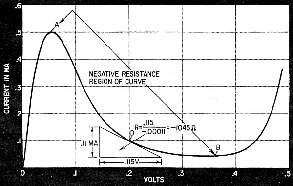
Fig. 1 - Typical germanium tunnel-diode characteristic.
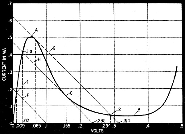
Fig. 2 - Tunnel-diode characteristic with load lines for 500-ohm resistor in circuit of Fig. 3.
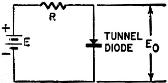
Fig. 3 - Basic tunnel-diode circuit.
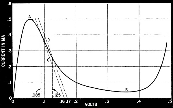
Fig. 4 - Tunnel-diode characteristic and load lines of switching property. Although related to the transistor, the tunnel diode operates upon a different principle and offers advantages not found in transistors. Some of these are its very small size, extreme speed and stability under varying temperature conditions. It is a new circuit element which may, with appropriate circuitry, function as a switch, amplifier and oscillator. Amplification and oscillation are possible well into microwave frequencies. At lower frequencies tunnel diode circuits may be simpler, smaller or more efficient than those of vacuum tubes or transistors. Let's see what this tunnel diode is and how it can be used in different circuit applications. This new device gets its name from a mechanism called "quantum-mechanical tunneling" (until now of only theoretical interest) which describes the manner in which electrical charges move through the device. The combination of this "tunnel effect" and the fact that the device comprises a p-n junction between two regions of very heavily doped semiconductor material has led to the name tunnel diode. Negative Resistance The property of the tunnel diode produced by the tunnel effect is the negative resistance which appears over a portion of its voltage range. A negative resistance may be defined as a circuit element in which current decreases with increase in voltage (or vice versa). This negative-resistance property is illustrated in Fig. 1, which shows the current-voltage characteristic of a typical germanium tunnel diode at room temperature. The negative-resistance region of the curve lies between points A and B. The slope of this curve at any point is the resistance of the tunnel diode at that point. A vertical region (infinite increase in current), for example, would indicate zero resistance while a horizontal region (no increase in current) would indicate an infinitely large resistance. In addition, a region which slopes upward to the right indicates a positive resistance while a region which slopes upward to the left indicates a negative resistance. An examination of the curve of Fig. 1 shows that the region from zero to A represents a positive resistance, the region from A to B represents the negative resistance and the region beyond B again represents a positive resistance. The current-voltage characteristic of the tunnel diode, therefore, has a region of negative resistance between two regions of positive resistance. While the tunnel diode is related to the transistor, the semiconductive material used is much more heavily doped with impurity than that used for transistors. It is almost metallic, and no hermetic seal is necessary for protection from such things as surface contamination and moisture penetration. A p-n junction formed between a heavily doped body of p-type conductivity and a heavily doped body of n-type conductivity semiconductive material is very narrow, about one-millionth of an inch or less. It is this combination, with the proper forward bias, that allows a "tunnel" current to flow and produces the negative resistance. All we need to know about this tunnel current is that its transit time is so short that it does not affect the maximum operating frequency of the diode. This frequency limit is set by the junction capacitance and negative resistance of the device and the bulk resistance of the material from which it is made. A diode was recently made to oscillate at 10,000 mc. However, for known materials, the calculated maximum frequency of oscillation is 20,000 to 30,000 mc. Now, how do we use the tunnel diode in a circuit? The current-voltage characteristic described above and shown in Fig. 1 is the key. Since the slope at any point of this curve is the resistance of the diode, this property of the diode may be conveniently determined from it. For example, the resistance at point D in Fig. 1 is 0.115/-0.00011 = -1045 ohms. Notice again that between A and B the diode is a negative resistance, that is, the current decreases with increase in voltage. At points A and B, however, the resistance is very high. We can see this on the curve itself. In the vicinity of A and B there is little or no change in current with changes in voltage. The locations of points A and B of the curve are set mainly by the semiconductive material from which the tunnel diode is made. For germanium, the voltage at A is typically about 0.05 volt and at B 0.3. For silicon, on the other hand, the voltages are 0.07 and 0.4, respectively. Other materials have somewhat different values. However, all are in the forward voltage range of less than 1 volt. Properties To understand how to use the tunnel diode in various circuit arrangements, it will be useful to first explore some of its electrical properties. It will be convenient, therefore, to refer to the simple series circuit arrangement of Fig. 3. Then, in conjunction with Fig. 2, we will analyze the operation of the tunnel diode.
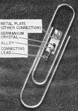
Laboratory style tunnel diode (original prototype). Semiconductor bodies are alloy and germanium crystal. A current-voltage characteristic of a typical tunnel diode is shown in Fig. 2 The current through it is shown with respect to the voltage Eo across its terminals. Since the circuit of Fig. 3 is a simple series arrangement, the voltage Eo at any time is equal to the battery voltage E minus the voltage drop in the resistance R. It would be very useful, therefore, also to know the current flowing in resistance R with respect to the voltage drop in it. Load line F in Fig. 2 shows just this relation and a very useful tool is available from it. The intersection of line F with the' voltage axis shows the battery supply voltage E while its intersection with the diode characteristic curve shows the voltage Eo. Load line F may be used to represent the resistance R in the circuit of Fig. 3. While the slope of this line is negative and it appears at first that there is a decrease in current with increase in voltage, it must be remembered that the load line F does not show the current flowing in the resistance with respect to the voltage supplied, as is the case for the diode characteristic. Rather, it shows the current flowing with respect to the voltage drop in the resistance. For this reason, this negative slope is not to be confused with the negative-resistance region (A-B) of the diode characteristic. The slope of load line F is determined by resistance R so that, having drawn a particular load line on the diode characteristic, one can easily find the resistance (R) necessary to establish it. For example, to find the R necessary to get load line F in Fig. 1, the slope is found from the voltage and current values taken from the curve. Line F's slope is equal to 0.1/-0.0002 = -500. The value of resistance R is +500 ohms since, as stated above, the negative slope does not concern us here. For the condition shown, E = 0.1 volt, Eo = 0.009 volt and the current is 0.18 ma. Therefore, with the above values, the point of operation of the diode (for the circuit of Fig. 3), will be as shown at 1 in Fig. 2. Although the slope of this load line is fixed by the resistance R in the circuit of Fig. 3, a change in the battery supply voltage will change its location with respect to the current-voltage characteristic. Now, let us increase the battery supply voltage. As this is done the load line moves up along the branch 0-A. When the intersection (or Eo) reaches a point near A, as shown by the load line G, the intersection (Eo) jumps almost instantly to the point 2 between Band C. Point 2 represents the new value of voltage Eo.
Fig. 5 - Characteristic and load lines illustrating amplifying property.
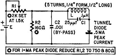
Fig. 6 - Tunnel-diode oscillator circuit. Values given are for 100-mc operation. Unit may be frequency-modulated by 2,000-ohm headphone across R2.
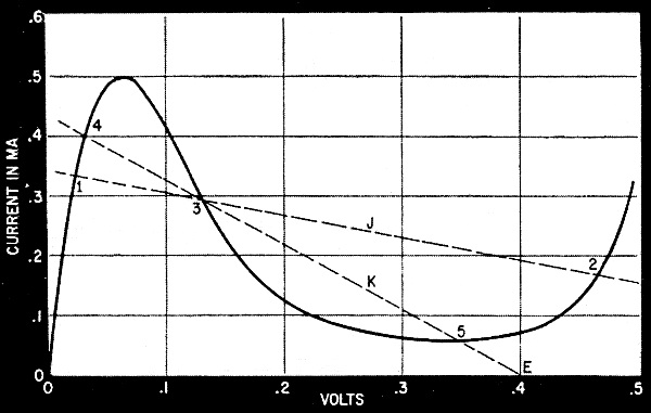
Fig. 7 - Characteristics and load lines illustrating oscillator operation. If now we decrease the battery supply voltage E, the load line and its intersection will move toward the point C. Here it switches suddenly to the-point 1-a on load line H and the lower value of voltage Eo. Notice that the slope of the load line remains the same, since resistor R was fixed at 500 ohms and only the position of the line along the voltage axis changes with change in battery supply voltage. Load lines G and H show the battery supply voltages as 0.314 and 0.235 at the respective switching points. This shows that, as the battery voltage E was increased from zero, Eo increased to 0.065 volt and then very suddenly switched to 0.29 volt. This is an increase in voltage across the diode (Eo) of 0.225 volt. Reducing the battery voltage to 0.235 volt then caused Eo to switch suddenly from a value of 0.155 to 0.03 volt. This is a decrease in voltage across the diode terminals of 0.125 volt. Thus, we see that near the switching points A and C a very small change in the battery voltage produced a relatively large voltage change across the diode. This property of the tunnel diode indicates one area of its usefulness. Switching Load line J in Fig. 4 (using the circuit of Fig. 3) represents a value of resistance much higher than the negative resistance of the diode. Notice that this load line intersects the characteristic in both positive resistance regions. Thus there are two stable operating points for a single battery voltage E. The voltage across the diode can be either that corresponding to point 1 or that corresponding to point 2. To show that only points 1 and 2 are stable, look at Fig. 4 and load line J. Now imagine for a moment that the current and voltage have values corresponding to point 3. If, for any reason whatsoever (motion of electrons, heat or anything else), there is a very small increase in the current, then by looking at the characteristic curve we can see that there must be a decrease in the voltage across the diode. A look at the circuit shows us that, if this happens, there is more voltage available to send current through the resistance which causes a further decrease in the voltage across the diode. This action continues until point 1 is reached. At point 1, however, if there is to be any further increase in the current, there must also be an increase in the voltage across the diode since this is a positive resistance region. The only way the voltage across the diode can increase, of course, is for the voltage drop in resistance R to decrease. And this is possible only if the current becomes smaller. The operating point then must remain at 1 and be stable there. The same thing would happen with any small decrease in current from that at point 3 so that the point would be then stable only at 2. This shows us that it is possible to provide a circuit arrangement which can be quickly changed from one impedance condition to another. For example, when the diode operates at point 1, it is in its low-impedance state and a relatively large current may flow. When operating at point 2, it is in a higher-impedance state and the current is limited to a relatively low value. Selecting a load line such as K in Fig. 4 with its corresponding battery voltage E will indicate how this change may be made more significant. For example, the current at point 4 on load line K for a germanium diode of about 0.5-ma peak current is 0.3 ma and the slope indicates an impedance of about 150 ohms. However, the current at point 5 is 0.055 ma and the slope indicates a very high impedance. Thus, the diode can be employed to switch impedances, currents or voltages if desired. To use the tunnel diode as an amplifier or an oscillator, we must prevent it from switching. When we look at the diode characteristic curve we realize that, for this to be done, the value of resistor R must be less than the negative resistance of the diode. That is, the load line established by resistance R must have a steeper (more vertical) slope than the slope of the negative-resistance region between A-B (Fig. 1). Such a load line is shown as C in Fig. 5. It always has only one intersection with the diode characteristic, making it possible to have an average bias in the negative-resistance region. The slope of region A-B for a typical germanium tunnel diode having a peak current at point A of about 1 ma is about -100. Hence its negative resistance will be 100 ohms. If now we choose a tunnel diode with a junction area 10 times as large (so that the peak current is 10 ma), we find that the slope of the region A-B is steeper and the negative resistance is reduced to only 10 ohms. From this we can see that, as the diode's peak current increases, resistance R must decrease to prevent switching.
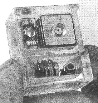
An FM transmitter built around a tunnel diode. The microphone is in the upper right corner and the battery is covered by it. The tunnel diode is to the left of the mike. Amplification Now how can the tunnel diode amplify? Refer to Fig. 3 again and assume that the diode is biased somewhere between the points A and Band has a load line such as shown at C on the characteristic of Fig. 5 so that it looks like a negative resistance. This negative resistance is indicated as (-Ro). Then: (1) eo = [e(-Ro)]/[R + (-Ro)], or gain = eo/e = (-Ro)/(R + (-Ro), where e is a small AC voltage in series with the battery and eo is the AC voltage across the tunnel diode. From equation (1) we see that the gain is 1 when R = 0 and increases to a very large value as R approaches (-Ro). This is shown graphically in Fig. 5. Lines C and D correspond to a resistance R of 150 ohms and battery voltages of 0.16 and 0.17 volts, or a change of 0.01 volt. At the same time we see that the voltage across the tunnel diode is 0.085 and 0.125 volt, respectively, or a change of 0.04 volt. Therefore, the gain = 0.04/0.01 = 4. We also see that, as the slopes of the lines C and D approach that of region A-B of the diode characteristic, the gain increases. Now let us consider the circuit of Fig. 6. This arrangement can function as an amplifier or an oscillator, depending on the resonant impedance of the L-C circuit. Assume first that R1 is adjusted so that the diode has a negative resistance, -Ro, and that R2 is smaller than Ro, so that we will prevent switching. If the resonant impedance of the L-C circuit is made greater than Ro, then the circuit will oscillate. If, on the other hand, the resonant impedance is less than Ro, the circuit will amplify. Fig. 7 shows the diode characteristic with the DC load line C established by resistances R1 and R2 and the AC load line D due to the resonant impedance of the L-C circuit in order for the circuit to function as an oscillator. An important thing in regard to this is that the amplitude of the oscillation will build up until the average negative resistance of the diode just equals the positive resistance of the circuit at the operating frequency. For our purposes, it is sufficient to know only that this means that the diode still has a negative resistance while it is oscillating. We can make further use of this by adding another parallel-tuned circuit, tuned to a different frequency, in series with the oscillator tank. This circuit "sees" a negative resistance. If its resonant impedance is slightly less than the impedance of the oscillator tank, it will amplify at this new frequency. We can add still another tuned circuit and use it as an amplifier also by following the same procedure. As an example, we have had a circuit operating, using a single tunnel diode, that was an RF amplifier (100 mc), an oscillator (110 mc) and a mixer and if amplifier (10 mc)! A few of the successful applications of the tunnel diode are as quartz-crystal controlled oscillators, utilizing the series or parallel resonance of the crystal; frequency-modulated oscillators; regenerative frequency dividers; counters; logic elements; amplifiers and combination oscillator-amplifiers. The list is growing daily. * General Electric Research Laboratory, Schenectady, N.Y.
Posted May 19, 2023 |
|

 By R. L. Watters* and J. V. Claeys*