All About IC's - What Makes Them Tick |
|
Integrated circuits (IC's) were newcomers to the world of electronics in 1969. Most people, it is probably safe to say, had no idea what an integrated circuit (IC) even was. At the time, many experienced design engineers - perhaps especially experienced design engineers - had no formal training on the fabrication of integrated circuits. After all, assuming an engineering student graduated at the age of 22 years old and was in 1969 say, 30 years old, he or she would have begun junior level classes about 12 years earlier - 1957 for the sake of argument. Given that Jack Kilby applied for the patent on his ground-breaking, world's first integrated circuit in 1959, there is no way those engineers would have had instruction on the matter. Therefore, articles like this one in Radio-Electronics served as an introduction to IC fabrication processes. The fact is, even though these days all engineers take courses on semiconductor physics and fabrication, most will never need to apply that knowledge any time in their careers. See Part 1, Part 2, Part 3, Part 4. All About IC's - What Makes Them Tick by Bob Hibberd Texas Instruments, Dallas, Texas Learn how solid-state integrated circuits are made - Part 1
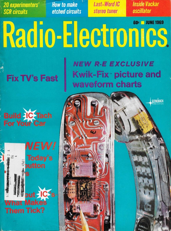
Fig. 1 - Electron and hole movement; forward bias (a) and reverse bias (b).
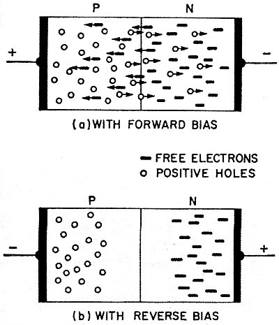
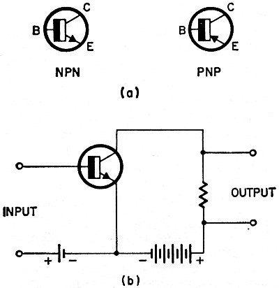
Fig. 2- (a) Diagram of npn, and (b) practical transistor arrangement. The potential of integrated circuits is so wide that in addition to replacing similar discrete component circuits, they are responsible for creating a completely new technology of circuit design. To get the full implication of integrated circuits, you must have a general basic understanding of solid-state technology and its application. We'll start with a general introduction covering the basic principles of solid-state semiconductor devices. Then we will review the processes used to form the solid-state structures used in integrated circuits. Basic Solid-State Principles In a conductor, electric current flow is a movement of free electrons. The outer or valence electrons of a good conductor such as copper are so loosely bound to the atom that at room temperature the thermal energy causes approximately one electron to detach from each atom and become free to move and result in a current flow when an electric potential is applied. Insulators are materials in which the outer electrons are tightly bound to the atom and no electrons are free to move. Thus, no current can flow when a voltage is applied. Between these two major categories is a class of materials called semiconductors. As the name implies, a semiconductor is a material with conductivity roughly midway between conductors and insulators. However, a semiconductor is not just a poor conductor; it has two other very important properties. First, its resistance normally decreases with increase of temperature, as opposed to conductors such as metals in which the resistance increases slightly with temperature. Secondly, flow of current in a semiconductor can be by two mechanisms, either by a flow of negative electrons similar to current flow in conductors, or by a movement of missing electron sites in the opposite direction. If an atom has one outer electron missing, a loosely bound electron from a neighboring atom can jump into it, leaving behind a new vacant site; this in turn can be filled by an electron from a third atom and so on. It then appears as if the vacant site has moved. Such vacant sites are called "holes" and since a negative electron is missing the hole can be considered as a positive charge. Semiconductor material in which conduction is by a flow of electrons is called n-type material (n for negative carriers) and material in which conduction is due to the movement of positive holes is called p-type. From the viewpoint of monolithic integrated circuits, the most important semiconductor material is silicon. Silicon has four outer or valence electrons. If we add a small amount of an impurity element with five valence electrons, such as phosphorus, one electron per impurity atom will be free and we have n-type silicon. Similarly, if we add an impurity with only three valence electrons such as boron, there will be one missing electron or hole per boron atom and we have p-type silicon. The operation of most solid state devices depends on the properties of one or more p-n junctions. A p-n junction is a transition from a p-type semiconductor to an n-type semiconductor within a piece of material. Alone, a piece of n-type or p-type semiconductor is purely resistive. Reversing a battery connected across it will reverse the direction of current flow, but will not affect the magnitude of the current. By contrast, a piece of semiconductor material with a p-n junction in it has rectifying properties. When the positive terminal of a battery is connected to the p-type side and the negative terminal to the n-type side, the free negative electrons in the n-type side are attracted across the junction to the positive contact, and the positive holes in the p-type side are attracted across the junction in the opposite direction to the negative contact (Fig. 1-a). This is called the forward or conducting direction. A high current flows with only a small applied voltage, and the forward resistance is very low. Now if the battery connections are reversed (Fig. 1-b) the holes in the p-type side are attracted away from the junction toward the negative terminal and the electrons in the n-type side are attracted away from the junction to the positive terminal and so no current flows across the junction. This is called the reverse or non-conducting direction and no current flows even with a high voltage applied. (In practice a very small leakage current does flow, due to free electrons and holes being generated near the junction by the thermal energy.) So a single p-n junction can be used as a rectifying diode.
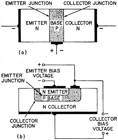
Fig. 3 - Common-emitter circuit has both the input and output common to emitter.
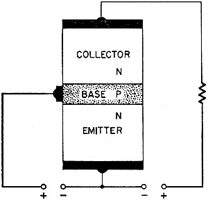
Fig. 4 - Symbols for npn and pnp transistors, and common-emitter circuit. An important point to observe is that when forward current is flowing through a p-n junction (Fig. 1-a) electrons are flowing through p-type material in which there are normally no free electrons, and also some holes are flowing through n-type material. The electrons are said to have been injected across the p-n junction into the p-type material. It is this situation that leads to the operation of the junction transistor. The NPN Junction Transistor A junction transistor consists of two p-n junctions formed in a piece of semiconductor material with a very small separation, only of the order of one-tenth of a mil. A diagrammatic npn transistor with its operating voltages is shown in Fig. 2. The first n-type region is called the emitter since it emits or injects electrons into the center p-type region which is called the base. The second n-type region is called the collector as it collects electrons from the base region. The junction between emitter and base is called the emitter junction and that between collector and base the collector junction. As mentioned above, in practice, the width of the base region is only of the order of a tenth of a mil. The collector junction is biased with a high voltage in the reverse direction (positive to the n-type collector, negative to p-type base) and so, considering the collector junction by itself, no current flows across it. Now suppose the emitter junction is biased in the forward direction (negative to the n-type emitter and positive to the p-type base). A forward current flows across the emitter junction and electrons are injected into the p-type base region. If there were no voltage applied to the collector junction, these electrons would flow out of the base contact, but with the collector reverse-biased, as soon as the electrons in the base region flow near the collector junction, they are attracted across it by the positive potential on the collector side. Thus most of the current crossing the emitter junction continues on across the collector junction. The current across the emitter junction was produced by a very low forward voltage (less than 1 volt) and this current now flows in the collector circuit, which is biased with a voltage, providing power amplification. As the electrons injected across the emitter junction flow through the base region, some of them fill holes in the p-type material. Thus the electron current crossing the collector junction is slightly less than the emitter current. The ratio of collector current divided by emitter current (IC/IE) is called the current transfer ratio and is designated by the symbol α, i.e. α = (IC/IE). A typical value for α is 0.98. A current equal to the difference between the emitter current and the collector current flows in the base lead so that IE = IC + IB, with α = 0.98, the base current IB will only be 0.02 times the emitter current. In the description of transistor action above, current through the collector is controlled by the emitter current, and the arrangement is called the common-base circuit since the base electrode is common to both input and output circuits. A more convenient arrangement is with the input fed to the base and the emitter common to both input and output as shown in Fig. 3. This is called a common-emitter circuit. The collector current is now effectively controlled by base current IB and the ratio of collector current to base current has a high value, equal to α / (1 - α). If α = 0.98 as above, (IC/IB) = α / (1 - α) = 49 Thus we have a current gain from the input to the collector of 49 times, and if the collector current flows through a load resistance to give a voltage output from the collector, a voltage gain results. The PNP Junction Transistor A pnp structure operates in a similar way to the npn transistor. There are two points to observe. First, to bias the emitter junction in the forward direction, the emitter must be made positive with respect to the base. To bias the collector junction in the reverse direction, the collector must be made negative with respect to the base. Secondly, the p-type emitter injects positive holes into the n-type base region, and they are subsequently attracted across the collector junction by the negative potential. To represent the transistor graphi-cally, the symbols shown in Fig. 4-a are used. The emitter is shown as an arrow pointing in the direction of positive current flow (opposite to the direction of electron flow). This device in a common-emitter circuit is shown in Fig. 4-b.
Fig. 5 - Crystal-pulling device uses seed crystal rotating in poly crystalline silicon. So far we have shown the importance of the pn junction. The technology of fabricating solid-state devices and integrated circuits has evolved around the development of methods of producing pn junctions in silicon material. The following sections are devoted to a general description of the basic processes involved in solid state technology. Silicon is a metallic element with a light gray appearance. It occurs in nature as silicon dioxide (silica) and as various silicate compounds. To prepare silicon for solid state devices, there are two main requirements. First, extremely high purity is required, with unwanted impurities down to a level of one part in 1010. Second, for a pn junction to operate as described earlier, the silicon must have a continuous regular crystal structure, and so the silicon must be converted into what is called single crystal form. The first step in the preparation of semiconductor grade silicon is to reduce silica by heating it with carbon (coke) in an electric furnace. The resulting silicon is about 98% pure. The next step is to purify this material. It is converted to a compound such as a halide (silicon tetrachloride) which is purified by repeated distillation. Then the purified halide is converted back to silicon by hydrogen reduction. In this process, the silicon is deposited onto the surface of a high-purity silicon rod, building it up to a diameter between 1 and 4 inches. Using this chemical method of purification, we get the required purity level of one part in 1010. The silicon deposits onto the rod in polycrystalline form and must now be converted to single crystal form. The process generally used to produce single crystal silicon for transistors and integrated circuits is called crystal pulling. The general arrangement is shown in Fig. 5. Solid polycrystalline silicon is placed in a pure quartz crucible supported inside a translucent quartz chamber, through which a flow of an inert gas such as argon is maintained. The quartz crucible is located in a graphite susceptor, which is heated by RF induction. When the silicon is all molten, its temperature is lowered to a value just above its melting point, and a seed crystal - a small piece of single crystal silicon - is lowered until it just enters the melt. The seed crystal is rotated (about 60 rpm) and slowly raised (about 1 inch per hour), growing larger as more silicon solidifies onto it. Typical pulled silicon crystals are cylindrical in shape between 1 and 2 inches diameter by about 12 inches long. The dopant to give n-type or p-type silicon is added to the silicon during the initial melting process so that the crystal has required conduction properties. Epitaxial Growth In the fabrication of solid state structures, we often want to form a thin film of single crystal silicon with certain conduction properties on the surface of another silicon slice. The process used is called epitaxial growth and films up to a few tenths of a mil can conveniently be formed. The starting slice must be single crystal with the required crystal orientation and is called the substrate.
Fig. 6 - Step-by-step photoresist process for removing selected silicon dioxide areas.
Fig. 7 - Fabrication of a silicon npn transistor using the diffused planar process. Hydrogen gas is bubbled through a volatile silicon compound such as silicon tetrachloride, causing it to vaporize. The mixture of vapor plus hydrogen is fed to a reaction chamber where the silicon substrate slice is heated to about 1200°C. The silicon tetrachloride dissociates and silicon is deposited onto the surface of the heated slice to form the epitaxial layer, which grows at about micron (0.04 mil) per minute. The conductivity of the epitaxial layer is controlled and arranged to be either p-type or n-type by introducing the requisite amount of a suitable dopant vapor into the hydrogen stream with the silicon tetrachloride vapor. Solid State Diffusion Solid state diffusion is a process involving the movement of n-type or p-type impurity atoms into the solid silicon slice. To do this, the slice is heated to a high temperature, between 800 and 1250° C, in the presence of a controlled density of the impurity atoms. In practice, the process is often carried out in two steps. The first step consists of heating the silicon slice in the impurity dopant vapor to form a high concentration of dopant on the surface. This step is called deposition. The slice is then removed to another furnace where it is heated to a higher temperature so that the dopant atoms on the surface move, or diffuse, into the silicon. This is called the diffusion step. If a p-type impurity is diffused into the surface of an n-type slice such that the density of p-type atoms then exceeds the original density of n-type atoms in the slice, the surface will be changed the p-type and a p-n junction will be formed a small distance in from the surface where the density of the diffuse p-type atoms equals the original n-type density. Convenient diffusant impurities for silicon are boron as a p-type impurity and phosphorus as an n-type impurity. A most important and significant fact is that a layer of silicon oxide on the surface of a silicon slice will prevent the diffusion of certain elements, including boron and phosphorus, into the silicon. Also important is that silicon oxide can readily be removed from the surface of the silicon slice by etching with a hydrofluoric acid solution without etching the silicon. Thus, if we oxidize a slice of silicon by heating it in a flow of oxygen to form a layer of silicon dioxide on the surface, and then remove the oxide from selected regions by etching, we can arrange to diffuse impurities into these selected regions only. This selective diffusion is the basis of all silicon monolithic integrated circuit fabrication - it allows the simultaneous formation of a number of separate components in a single slice of silicon. The selective removal of silicon dioxide is carried out by a photolithographic process using photoresist material. The several steps in the process are illustrated in Fig. 6. After oxidation (a), the oxidized surface of the slice is coated with a thin layer of photoresist lacquer (b). This is an organic substance which polymerizes when exposed to ultraviolet light, and then, in that form it resists attack by acids and solvents. A photographic mask, with opaque regions located where it is required to remove the silicon oxide, is placed over the slice and illuminated with ultraviolet light (c). The photoresist under the opaque regions of the photomask is unaffected and can be removed with a solvent, the exposed photoresist remaining in the other regions. The slice is baked to harden the photoresist and then immersed in a hydrofluoric acid solution to etch away the silicon oxide where it is not protected by the polymerized photoresist (d). Finally the photoresist is removed from the surface (e), and the slice is thoroughly washed. It is now ready for diffusion which will only occur through the openings (sometimes called "windows") in the oxide. This complete photoresist pro-cess must be repeated each time the silicon oxide is selectively removed. The Planar Process The combination of oxidation, selective oxide removal and diffusion forms the basis of the planar process, which is now firmly established as the basic process of solid state technology. The sequence of processes used to fabricate a silicon planar n-p-n transistor will be described in some detail. The processes are carried out on whole silicon slices, about 1.5-inch diameter by 10 mils thick. Each slice normally contains a large number of individual device patterns, and at the end of the slice processing it is cut up into individual wafers. Referring to Fig. 7, an n-type silicon slice is oxidized (a) and windows for the base diffusion are opened in the oxide (b) by the photoresist process as in Fig. 6. Boron is used as the p-type impurity for the base diffusion. Boron tribromide, a liquid, is vaporized, the vapor mixed with nitrogen, and passed over the silicon slice heated to a temperature of 850° C. During this process boron is deposited onto the surface of the silicon. The slice is then transferred to another furnace and heated at 1150°C in a flow of nitrogen for a sufficient time (about one hour) for the boron to diffuse in and form the p-n junction at the required depth. During the latter part of this diffusion, steam is mixed with the nitrogen so that a new layer of silicon dioxide forms on the surface of the diffused region (c). In addition to diffusing down into the silicon, the boron also diffuses sideways, and so the p-n junction is formed under the oxide and is protected against surface contamination. This is a very important feature of the planar process. A typical base diffusion depth is 0.1 mil.
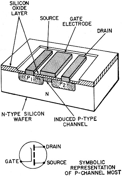
Fig. 8 - Semiconductor structure of MOS transistor and symbol for p-channel type. The slice is now prepared for the emitter diffusion by etching windows in the new oxide grown over the base region (d), using the identical photoresist process as before. To form the n-type emitter region, phosphorus is diffused in. Liquid phosphorus oxychloride is vaporized and passed over the slice at 1000°C. This is usually a single step diffusion, and for the latter part of the cycle, steam is again introduced to form silicon oxide on the surface (e). The emitter diffusion depth is about 0.06 mil, resulting in a base width between the collector and emitter junctions of 0.04 mil. The next process is to form metallized contacts to the base and emitter regions. Once more the photoresist process is used and contact windows are opened in the silicon oxide (f). Aluminum is now evaporated onto the whole surface of the slice, and a fourth photoresist sequence carried out with a "reverse" contact photomask to remove the aluminum from everywhere but in the contact windows. The aluminum remaining in the contact windows is then alloyed to the silicon to form a low resistance contact (g). Finally the slice is cut into individual transistor elements by scribing between the rows of elements and breaking into wafers. The individual wafers are assembled into transistor units by fusing down to a header, which forms the collector contact, and bonding connections to the base and emitter contact areas (h). It will be seen that all of the above processes are carried out on the top surface of the slice, and the three regions of the transistor - the emitter, base and collector - all come to this same plane surface and hence the name "planar." By changing the photomask details only, any size and shape can be given to the diffused regions, and so any desired element can be produced with the same basic diffusion processes. MOS Transistors
Fig. 9 - Nine steps used in the fabrication of the metal-oxide-silicon transistor. So far, we have discussed only the "bipolar" junction transistor - bipolar because two types of carrier, the free electron and the positive hole, are involved in its operation. A more recently developed transistor, the metal-oxide-semiconductor field effect transistor (the MOS transistor) is of considerable importance in integrated circuits. The basic operation of this transistor is quite different from that of the bipolar transistor. In it, a conducting channel is induced between two very closely spaced electrode regions by increasing the electric field at the surface of the semiconductor between the electrodes. The basic structure is shown in Fig. 8. The two electrode regions, called the source and drain, are formed by a p-type diffusion into an n-type silicon wafer. Between the source and drain are two pn junctions back to back, p1n and np2. With a voltage VDS applied between the source (positive) and the drain (negative), the np2 junction is reverse-biased and so no current will flow from source to drain. If now the gate electrode over the space between source and drain is made sufficiently negative with respect to the source, holes are attracted to the surface of the n-type region and cause it to change to p-type. Then we have two p-type electrodes with a p-type channel joining them and so a current can flow. The steps in the fabrication of an MOS transistor are shown in Fig. 9. An n-type silicon slice is oxidized (a) and a photoresist sequence used to form a window in the oxide for the complete device (b). Now a new thin layer of oxide is formed in the window by oxidation in steam (c) and a second photoresist process used to open windows for the source and drain diffusion (d), and boron is diffused in (e). The thin oxide is then removed by immersing the slice in a hydrofluoric acid solution (f). Next a new very pure oxide layer is grown over the device region (g) and contact windows for the source and drain opened by another photoresist process (h). Finally aluminum is evaporated over the whole slice and removed everywhere but in the source and drain contact windows and in the gate electrode region by a fourth photoresist process (i). The thickness of the pure oxide under the gate electrode is only of the order of 1000 angstroms and the spacing between the source and drain is typically 0.3 mil. The whole structure can be fabricated in an area about 3 mils by 1.5 mils and this makes the MOS transistor very suitable for use in integrated circuits where a high density of elements is desired. The fabrication of the MOS transistor in integrated circuits will be discussed in detail next month. R-E
Posted September 4, 2018 |
|