Four-Layer Diodes & Controlled Rectifiers - What Are They?
|
|
Stop me if you've heard this story before. Back in the early-mid 1980s I worked as an electronics technician at the Oceanic Division of Westinghouse, in Annapolis, Maryland. There was an older engineer there that dated back to the days of vacuum tube design who - and I'm not making this up - thought that a transistor could be made by connecting diodes together so their circuit resembled the NPN or PNP junctions inside a transistor. That is, connect the diodes anode to anode or cathode to cathode, respectively. He was amazed to learn of how the transistor actually worked. If I recall correctly, it wasn't long thereafter that he retired. This "Four-Layer Diodes & Controlled Rectifiers" from a 1961 issue of Radio-Electronics magazine would have really had him confused with three PN junctions rather than only two. To be fair, though, there are very few engineers using solid state devices that could tell you how to bias a vacuum tube. Four-Layer Diodes & Controlled Rectifiers - What Are They?
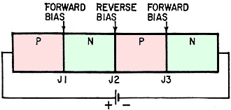
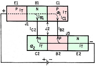
By Gene Jackson During the last decade, transistor development has progressed rapidly and received world-wide publicity. This is as it should be, but other developments in the semiconductor field should not be neglected. Some of these devices promise to play a very important part in the electronics of the future. Two examples are the four-layer diode and a modification of this basic device - the controlled rectifier. The author wishes to thank the Public Relations Div. of Texas Instruments Inc. for its permission to use data from the May 1960 issue of Application Notes as a source of information for material in this article. Many of the circuits discussed were constructed and results verified in the Training Aids Laboratory of the Educational Services Section of Convair, a Division of General Dynamics Corp., Fort Worth, Tex. The ordinary junction diode consists of a layer of P-type crystal joined to a layer of N-type crystal. It can be forward- or reverse-biased. With forward bias, the P-type material is made positive with respect to the N-type and the diode conducts. When the diode polarities are reversed, reverse bias results and very little current flows. The four-layer diode has two N-regions or layers and two P-regions as shown in Fig. 1. Under normal operating conditions, the center p-n junction is reverse-biased and the outer p-n junctions are forward-biased. To illustrate the effects of this arrangement, an equivalent structure is shown in Fig. 2. Here, a four-layer diode is represented by two transistors connected as shown. Notice, too, that the p-n-p transistor is correctly biased. The emitter-to-base junction (J1) is forward-biased and the collector-to-base junction (J2) is reverse-biased. Bias conditions occur in the n-p-n section are also correct. It is shown that IB1 equals IC2 and IC1 equals IB2. If this unit can be caused to begin conduction and increase the current through it to a certain critical point, this internal feedback mechanism sustains conduction.
Fig. 1 - Structure of a 4-layer diode.
Fig. 2 - Equivalent diagram shows two transistors connected to form a 4-1ayer diode.
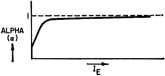
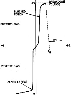
Fig. 3 - Alpha vs. emitter current for a 4-layer diode. To explain this, we can further state that any transistor has a value of alpha (α). This is indicated by: α = IC/IE (disregarding minority carriers) Or: IC = αIE Alpha is the portion of the majority carriers leaving the emitter and reaching the collector. In an ordinary transistor, alpha is made as large as possible to get the highest forward-current transfer ratio or current gain. Referring again to Fig, 2, the majority carriers in an n-p-n transistor are electrons. This is shown by the solid arrow. Because the majority carriers in the p-n-p section are holes and they move from positive to negative polarities, this current flow is shown by a dashed arrow. The current crossing J2 is α1IT + α2IT. Because of minority carriers, we cannot ignore the value of ICBO or reverse current present to some extent in all semiconductor devices. Therefore the total current across J2, which is actually the current through the entire device, can be shown as: IJ2 = IT = α1IT + α2IT + ICBO And: IT(1- α1 - α2) = ICBO IT = (ICBO)/[1 - (α1 + α2)] This indicates that if α1 + α2 equals unity, the current in the diode is limited only by the external circuit. If α1 and α2 are close to zero, the current through the diode is approximately equal to ICBO. Because J2 is reverse-biased and base current from both equivalent transistors must in some way cross this junction, there is only this leakage current available unless some method is found for "triggering" the unit. This nonconducting condition of the four-layer diode is the "blocked" state. Some method must be found to increase alpha if this device is to be useful. Two methods are generally used. One is to increase emitter current directly; the other is to increase the collector voltage and thus indirectly the emitter current. As in ordinary transistors, alpha or current gain increases with emitter current. Fig. 3 is a curve of alpha vs emitter current. If the voltage across the entire unit is increased to a certain critical point, the center junction, J2, breaks down (triggers) and allows reverse current to flow through it, and thus emitter current and alpha increase. The effect of this phenomenon is that the diode continues to conduct even if the high breakdown voltage is decreased. The device has switched from its "blocked" condition to its "on" condition. It will remain in this state as long as the current through J2 is great enough to cause α1 + α2 to be equal to unity. The current at this time is limited almost totally by the voltage applied and the resistance in the external circuit, as the resistance of the diode is now extremely low. The minimum current that must flow through J2 and also in the external circuit to maintain this "on" condition is called the holding current, IH.
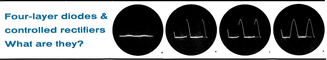
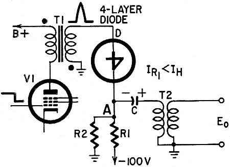
Fig. 4 - Forward-bias voltage vs. current for a 4-layer diode. This plot of forward-bias voltage current is in Fig. 4. If the polarity of the voltage across the diode is reversed, J1 and J3 are reverse-biased and J2 is forward-biased, The effect then is similar to two reverse-biased diodes in series. As shown in Fig. 4, the unit then acts like any reverse-biased diode. If the voltage reaches the breakdown point or Zener voltage, current through the device increases. However, the voltage across the diode does not decrease, and it could be used for voltage regulation. This is not, however, its most useful application. Typical Application Perhaps a discussion of a typical application of this diode would be useful in pointing up its possibilities. Fig. 5 is a partial schematic of a circuit using such a diode. In Fig. 5, R1 and R2 act as a voltage divider across the negative 100-volt supply so that approximately -60 volts appears at point A. As the break-down voltage of the four-layer diode is 80 volts, it does not conduct until additional voltage is applied across it. When a negative-going signal is applied to V1's control grid, a positive pulse of over 20 volts amplitude appears at V1's plate and across T1's secondary. This increases the potential difference across the diode past 80 volts and it conducts. At this time the resistance and the voltage drop across the diode become very low. Effectively, the secondary of T1 and C, which is charged to the polarity shown, is applied directly across T2's primary. Thus, a pulse of slightly more than 20 volts results in a signal of more than 80 volts across T2's primary. Although the four-layer diode cannot be called an amplifier in a true sense, it actually amplifies the input signal. The diode will very shortly block or go to a nonconduction state because, when C has discharged and the trigger input at T1 has elapsed, there is not enough current (IH) to hold D in a conducting state. R1 is chosen so that D's IH is greater than the current through R1 with a 100-volt drop across it. The circuit then recovers, C again charges to the polarity indicated and another input pulse may be applied. Controlled rectifier in circuit of Fig. 8 produces these scope patterns: a - R1 set for zero gate current. There is no anode current. Low-amplitude waveform is result of minority carriers only. b - IG is large enough to cause some conduction, but not during the entire positive alternation. c - A still higher value of IG causes this waveform, d - VG has been advanced until the firing point occurs very early in the half-cycle.
Fig. 5 - Possible circuit uses 4-layer diode switch.
Fig. 6 - Controlled-rectifier construction and 2−transistor equivalent arrangement. The Controlled Rectifier Another method of turning this type of device "on" without reaching the breakdown voltage across the diode is used in the controlled rectifier. A structure diagram of this unit is in Fig. 6. Fig. 6-a shows the necessary electrical connections and polarities. Fig. 6-b is the equivalent structure diagram. When operating below the breakdown voltage, the device is in its blocked state and only ICBO flows in the circuit. However, we have now added another connection to this modified four-layer diode or controlled rectifier - the gate lead connected to the center P-region. If a positive voltage is applied to the gate lead, current flows in this part of the circuit as this represents forward bias for J1. Because of transistor action, some of the electrons from the cathode drift across the first P-region (actually the base region for the equivalent n-p-n transistor) and enter the second N-region by diffusing across J2. Because J3 is forward-biased, electrons and holes combine in the area of J3. This results in electrons leaving the anode circuit from the top P-region and causing holes to form here. Thus, current has been increased through the device. Furthermore, as the holes formed near the anode lead drift across the P-region and cross J3, some combine with electrons from J2 and some diffuse across J2 and enter the next P-region. Transistor action has now been accomplished in both equivalent transistor sections. As the current through the device is thereby increased, alpha or current gain of both sections increases. This results in further increase in current and alpha until the unit saturates. We have seen that, once the gate current reaches a certain point, the device turns "on" and the current through the controlled rectifier is limited only by the voltage and resistance in the external circuit. This is similar to the action of a thyratron where the grid voltage controls the firing point. The controlled rectifier has the advantage of a very small voltage drop across it when conducting. This means that a controlled rectifier can be used where a thyratron might be impractical.
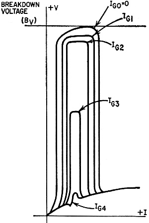
Fig. 7 - Effect of IG on anode current for a controlled rectifier. Another advantage of this arrangement is that a small gate current, IG, can cause a large change in anode current. This action is shown graphically in Fig. 7. If there is no gate current, the voltage across the device must be increased until the breakdown voltage is reached to cause the device to turn "on". The current then increases and the voltage across the unit is small. As the gate current is increased, the controlled rectifier will fire with less voltage across it. This is indicated in Fig. 7 where IG0<IG1<IG2<IG3<IG4. Demonstration Circuit A simple circuit that can be used to demonstrate the characteristics of the controlled rectifier is shown in Fig. 8. A Texas Instruments 2N1595 controlled rectifier diode is used. If a rectifier with high enough breakdown voltage . (BV) and power dissipation ratings is used, the transformer may be eliminated and the line voltage connected directly across D. Be sure that the maximum permissible gate current is not exceeded at any time. With R1 set for zero gate voltage, there is no anode current. This is shown in Fig. 9-a. The low-amplitude waveform is the result of minority carriers only (ICBO). The scope's vertical gain had to be increased for this photograph so this conduction would show up. As potentiometer R1 is adjusted so that gate current flows, a point is reached where the diode begins to conduct on part of the forward voltage alternation. This is because, with a higher gate current, the rectifier turns "on" with a smaller forward voltage. Fig. 9-b shows a condition where 10 is large enough to cause some conduction, but not during the entire positive alternation. Fig. 9-c illustrates a still higher value of IG. R1 can be adjusted to change the firing point while observing the result on the oscilloscope. As VG is increased, the firing point occurs earlier in the half-cycle until the waveform of Fig. 9-d results. This is a typical half-wave rectifier output. Notice that, if the firing does not occur on the positive-going portion of the positive alternation, it does not occur during the negative portion as the voltage across the rectifier is now decreasing. There is a small irregularity in the extreme lower trailing edge of the rectifier output. This is caused by the current through the rectifier dropping below the holding current of the device.
Fig. 8 - Demonstration circuit using a controlled rectifier. The controlled rectifier must be turned "on" again during each positive alternation as it will "block" during each negative alternation and the entire process is thereby repeated. An interesting variation of this circuit is to substitute an alternating-current source for the battery. If the gate goes positive at the same time as the anode, the unit conducts. If not, the device remains cut off. This suggests many possibilities of using the p-n-p-n controlled rectifier as a phase detector or servo system control device, etc. As the electronics industry becomes more aware and informed of p-n-p-n rectifiers, many additional applications will be uncovered. The uses of controlled rectifiers in the future are limited mainly by the imagination and ingenuity of designers. Controlled rectifiers are already being used in control circuits, pulse-generating systems switching circuits and other such applications. As the state of the art is extended, more and varied circuit functions using these devices will be coming into general use.
Posted August 17, 2023 |
|