Understanding Solid-State Lasers
|
|
It is safe to say that all realms of semiconductor technology have advanced significantly since the 1970s. Gate widths, wafer purity, doping compounds, feature dimensions, layer stacking, power handling, operational frequency, physical and electrostatic discharge (ESD) ruggedness, cost, reliability - like I said, all realms - have improved. Laser diodes were a major development due to lower cost, compactness, spectral purity, and lower operational voltage, as compared to lasers built from rare earth elements and noble gases. Of course a solid state laser will never (probably) be able to shoot an inbound ICBM out of the sky, but the vast majority of laser applications today require only micro- or pico-power. Optical media read / write devices alone comprise a huge fraction of the low power laser market. Modern laser diodes are employed in, among other things, chemical analysis, range measurement, motion / position sensors, and even play toys for cats and dogs. Solid State columns: April 1967, August 1967, April 1966, August 1970, July 1971, October 1971, April 1972. Understanding Solid-State Lasers
By Forrest M. Mims Would you believe that there are lasers smaller in size than the proverbial grain of sand? Well, semiconductor lasers like the one in the photo at left have been around since 1962; but few people have even heard of them. This tiny laser promises to make important contributions to communications, crime prevention, and even ultra-fast computers in which wire interconnections are replaced by beams of light. Like all other new arid specialized electronic components, these lasers are relatively expensive; but a recent price cut by one major manufacturer makes the semiconductor laser by far the least expensive of all lasers and entirely within the budget of many electronics experimenters.
In this typical laser diode chip, a gold layer is usually evaporated over an insulating layer of transparent silicon monoxide on the rear reflect - or to collect light more efficiently. The history of the semiconductor laser is filled with difficult technological and theoretical accomplishments - flavored with a dash of serendipity. Even before Theodore Maiman's first ruby laser was constructed in 1960, physicists had made predictions about the possibility of laser action in a semiconductor. In the late 1950's and early 1960's, rapid advances were made in the development of semiconductor light-emitting diodes (LED's) and most scientists working in the field realized that laser action was within reach. In 1962 a Soviet researcher reported that the output of an LED became purer when the diode was stimulated by very high current pulses. This was an important clue since theory had not predicted the very high current levels which would eventually be needed for true laser action in a semiconductor diode. Researchers at several important laboratories went right to work in a highly competitive race to develop the first laser diode. In the fall of 1962, GE, IBM, and MIT all announced the development of lasers made from specially modified LED's. The laser diode development immediately touched off a major research effort. Since the laser diode converted electricity directly into light, it was far more efficient than any other laser at that time. And, even now, only certain types of gas lasers are more efficient. The first diode lasers were made from gallium arsenide (GaAs); and, though lasing has been observed in numerous other semiconductors, nearly all semiconductor laser research centers around this material. Diodes are commonly used, but since some semiconductors cannot be given a junction, bulk material is sometimes bombarded by high energy electrons to produce laser action. This technique can result in beams of intense visible light. Since GaAs lasers normally emit in-frared and must be operated at very low temperatures to produce visible light, there is strong interest in materials which produce visible light at room temperatures. Both GE and IBM went on to produce commercial lasers for civilian and military applications, but RCA has made perhaps the biggest contribution to the field. Having had considerable experience with GaAs (as a result of years of work with radiation resistant solar cells and tunnel diodes) RCA was in an excellent position to jump into the laser field, and they perfected new techniques for fabricating efficient solid-state lasers. General Electric eventually dropped out of commercial production due to the limited market, but RCA and IBM have competition now in the form of several other laser producing companies.
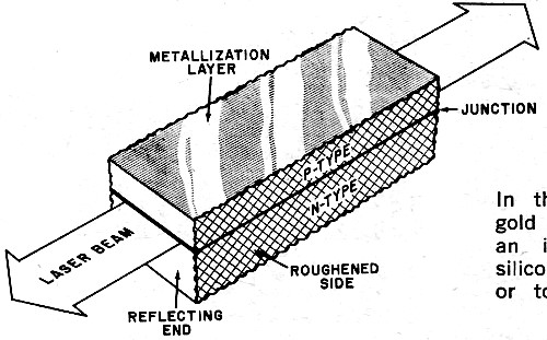
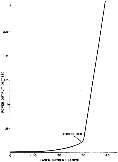
The light output versus current input of a typical laser diode looks like this plot. The extremely abrupt increase in light output makes it easy to identify the actual lasing threshold. How They Operate. The LED readily emits light when stimulated by very small amounts of electricity. In the case of the laser, we require that such a medium be placed between two mirrors to fulfill a fundamental requirement for laser action. So, why can't we fabricate an LED so that it has two parallel mirrors? We can - very conveniently - since the index of refraction of most semiconductors is sufficiently high that their surfaces act as partially reflecting mirrors. GaAs is a crystal and since a crystal cleavage surface is very flat and they can be made parallel to each other, it is very easy to make a GaAs LED into a laser diode merely by cleaving two opposite sides. It is actually very easy to cleave GaAs and the operation is often accomplished with nothing more than a razor blade; but for many reasons, the process used is not that simple, so fabrication becomes an important subject. Fabrication of Laser Diodes. The LED can be a very simple device. In fact, even a conventional silicon or germanium diode will produce infrared light - though very inefficiently. GaAs LED's are often merely a wafer of p-type material into which has been diffused a thin layer of n-type material. Light emission occurs at the junction of the p and n layers when electrons, propelled over the junction barrier by the diode's forward voltage, fall back to their normal unexcited state. In the process, most of the electrons give up a good deal of their stored energy in the form of light. Although this process of light generation is basic to the diode laser, its fabrication is far more specialized. Before the GaAs crystal is cleaved to form the parallel, reflecting sides, it is prepared in wafer form. Very thin wafers which have been sliced from the bulk crystal by a diamond saw are given a pn junction by either the diffusion or epitaxial process. In the case of diffusion, an n-type wafer is baked under carefully controlled conditions in the presence of zinc or other p-type materials. After a suitable period, the wafer is removed from the furnace, cleaned, and metallized on both sides with tin, gold, or some other contacting material. The metallizing process is the same for epitaxial lasers, but the junction formation process is far different. There are several techniques; but usually the wafer, after being brought to a high polish, is immersed in molten p-type GaAs. A very thin section of the polished surface melts and, when the furnace is slightly cooled, a layer of GaAs literally grows on the wafer. The process results in extremely uniform pn junctions - a very important factor in the operation of the diode laser. The fabrication process from here on is very similar for both diffused and expitaxial lasers. Cleaving is accomplished with a razor blade or by scribing parallel lines across the wafer with a sharp instrument and then rolling a glass rod over the wafer. Gentle pressure applied to the rod results in the formation of a series of long bars with parallel sides. After cleaving, the individual bars are coated on one of the two parallel sides with a layer of silicon monoxide and gold, the former for insulation, the latter for 100% reflection. Next the bars are separated into individual chips, typically between 3 and 50 mils wide. The separation can not be done by cleaving as this would result in four parallel surfaces - a condition which tends to quench laser action. So usually chips are made using a diamond or wire saw.
As shown here, typical laser output is composed of many very narrow spikes that make up total width. Individual chips are cleaned and then soldered to the heat sink block of a special header. The chip can be soldered to the block and given a positive electrode at the same time. A technician orients the header in a jig under a microscope so that the block faces up and then puts a tiny square of tin on the heat sink. Next come the laser chip, another square of tin, and the wire electrode. A drop of flux is added and then heat is applied. As soon as the tin begins to melt, the heat is turned off and the laser is ready for installation of a protective cap - with a glass window. In another fabrication process used by some companies, an indium plated chip is pressed between two similarly plated copper strips. The soft indium provides good thermal and electrical contact. Lasers produced in this manner are sometimes difficult to work with, but their excellent heat sinking characteristics permit much higher duty cycles than lasers mounted on a header. Since it takes time to saw individual laser chips from GaAs bars, saws with as many as 75 wires are often used. Not only does this result in an important production shortcut, it also facilitates the fabrication of arrays of lasers. Normally a single chip is affixed to a header as described above, but if a great deal of optical power is required, a large number of chips will be needed. Rather than use many separate laser containers, manufacturers often attach a long bar of GaAs with its built-in diode junction to a substrate, saw it (but not the substrate) into separate chips, and connect the chips together in series with tiny wires. The technique provides a sturdy array of as many as 75 lasers which can be put in a package not larger than an ordinary transistor. Such an array may produce 300 or more watts of peak optical power! For applications where even more power is required, such as in covert illumination systems for the military, a dozen or more array strips may be used. How They Operate. Now that we have a laser diode, or perhaps a laser array, how is it operated and what are the characteristics of the emitted light beam? Nearly all other types of lasers are stimulated into laser action indirectly. A very attractive feature of the diode laser is that it can be driven directly and efficiently by an electrical current. Though Bell Labs has very recently developed a laser diode which can be operated continuously at room temperature, the lasers available to us now must be operated only in a pulsed mode to prevent catastrophic destruction. A typical laser diode may be operated at a repetition rate of up to 10 kHz with an absolute maximum width per pulse of 0.2 microseconds. Since the laser diode requires relatively high currents, the design of a suitable pulse generator can be a little tricky. Due to their very fast switching characteristics, SCR's, avalanche transistors, and miniature thyratrons are often used. Since very fast pulse rise times are essential for efficient operation, lead dress is fairly critical. Several things happen when a single pulse is applied to a laser diode. At first, incoherent light is emitted and the chip acts as an LED. As the current increases and reaches the lasing threshold, laser action suddenly begins. An examination of the beam pattern would reveal a bright distinct pattern on a surrounding field of relatively uniform light. The uniform field represents the incoherent output of the laser and remains relatively constant. The distinct pattern becomes extremely brilliant as the current pulse continues to rise to the peak. However, another interesting thing is going on: the chip is heating up. Since the output is directly related to chip temperature, the wavelength begins to shift. For a typical laser operating at room temperature, the shift in wavelength is about 2.5 Angstroms per degree Centigrade. Since the temperature of a chip may rise about 2°C during a single pulse, the wavelength may shift 5 Angstroms. As the current pulse reaches a peak and begins to decrease, the threshold value is again reached and the light output drops sharply. Below threshold, the chip again functions as an LED. While the pulse drive recycles for the next pulse, the laser literally cools off in preparation for it.
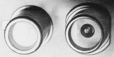
Two styles of laser diodes. The RCA version (right) includes heat sinking and mounting. Lasers vs LED's. Just what does the laser have over the LED? Because of the stringent requirements imposed on the operation of the diode laser, it may appear that the LED can do the same job with less trouble. Often this is true. For example, in communications, the LED is presently far more efficient than the laser. Also, in any application that requires a continuous beam or a pulse longer than a few tenths of a microsecond, the LED is a must. Still another plus for the LED is that relatively slow photo transistors can be used to detect the beam. Since the laser diode output is such a very brief pulse, efficient de-tection requires a fast photodetector. While readily available, these devices are generally much less sensitive than phototransistors. But there are certain overwhelming advantages that make the laser diode a must for some important applications. First, the output power of a single laser diode is easily more than 1000 times that of the LED on a pulse-for-pulse basis. While both devices, in general, have about the same average power, the high peak power of the laser makes it very attractive for pulsed applications such as ranging. Another significant factor in favor of the laser is the extremely small size of the chip. Since light is emitted from a spot only a few microns thick and from 3 to 50 thousandths of an inch wide, it is very simple to focus it into an extremely narrow beam. A simple convex lens with a focal length and diameter of about an inch will produce a beam which diverges only a fraction of a degree. Narrow beams are important for communications over long distances, range finding, and covert illumination. Applications. Communications and ranging are perhaps the most promising applications for the diode laser. The recent development at Bell Labs of the diode laser which operates continuously at room temperature is a major step forward in communications since total utilization of the diode laser's properties requires a continuous source. For more limited communications and ranging, a pulse laser is perfectly adequate. In ranging, for example, a very brief pulse of laser light is sent toward a distant object whose range is unknown. At the same moment, a high-frequency counter is activated. When a sensitive detector circuit on the unit receives the reflected pulse, the counter is deactivated and the range is read directly from a digital display. Another use of the pulsed laser diode is in mobility aids for the blind. LED's have also been used for this purpose, but the laser offers several advantages. Since the laser is such a tiny source of light, it is very easy to focus its output into a narrow beam with a very small lens system. With its high peak power and narrow pulse width, the laser makes for a very sensitive, noise immune system.
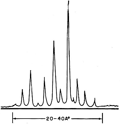
Laser diode chips are soldered to heat sink blocks within the header. Actual size of header is similar to that for transistors. Reflected light for the camera obliterates the chip in device on the left. A very important potential application of laser diodes will be as active elements in an optical computer. When one laser is illuminated by another, extremely rapid switching effects are observed. For example, various types of gates can be made by fabricating several lasers in a single GaAs chip. If the lasers are properly arranged and appropriate contacts are applied, switching speeds of well under a nanosecond can be obtained. In fact, the switching speed of the laser is so rapid that it is difficult to design circuitry with which to exploit it. A laser application which has resulted in a large number of military contracts - and consequent advances in the state of the art - is covert illumination. In conjunction with image converters (devices which make infrared light visible to the human eye) powerful laser diode searchlights are important battlefield devices. Over a thousand individual laser chips may be used in an illuminator, which is artificially cooled to permit operation at a high duty cycle with a resultant increase in average power of up to 30 watts or more. A commercial application of the laser diode is in intrusion alarms, The narrow beam characteristic of the focused laser permits long path lengths to protect large areas. Physics of Laser Diodes An essential requirement for a laser is two mirrors, one on either side of an optically active medium. The process of laser action begins when electrons in the active medium are excited to a higher than normal energy level by the application of optical or electrical energy. The electrons have a tendency to remain at the higher level for a brief period of time, and then they begin to fall back to their normal level, in the process giving off the energy absorbed from the excitation source in the form of heat or light. If photon emissions predominate and if a very large number of electrons are in the excited state, a condition will exist where an emitted photon from one electron may stimulate the emission of a photon from another. This process, which obviously can become a chain reaction, is called stimulated emission of radiation. Since the active medium is between two facing, parallel mirrors, a feedback mechanism is provided to encourage the stimulated emission of very large numbers of photons. Like water sloshing back and forth in a basin, the oscillating photon beam quickly builds in intensity until a portion penetrates the more transmissive of the two mirrors. This process of light generation occurs in one form or another in all types of lasers. But a full understanding of the laser diode requires a consideration of electrical and optical properties. A detailed explanation of the generation of light in a semiconductor will be found in the November 1970 issue of Popular Electronics. Briefly, light is generated in some types of semiconductor diodes when electrons which have been raised to a higher than normal energy level in order to penetrate the junction fall into holes. Since the laser diode has semi-mirrored ends, the essential requirement for laser action is realized and a quasi-coherent beam of light is emitted from the junction region. Because the junction is very thin, the light is far more divergent than the beam produced by most lasers. The spreading is identical to that which occurs when any beam of light passes through a narrow slit and is diffracted outward. While the GaAs LED emits a fairly uniform spectrum of light about 300 Angstroms wide, the spectral output of the GaAs laser usually consists of an envelope of extremely narrow spikes. Total width of the envelope is 20 to 40 Angstroms, but individual spikes may be extremely narrow. The spikes result from definite optical modes within the laser and indicate, as does other evidence, the existence of some coherence in the emitted beam. But, unfortunately, the laser diode is not nearly as coherent as most other lasers. Though the discussion so far applies generally to all GaAs laser diodes, various junction formation techniques can cause a wide variation in device efficiency, current requirements, and lifetime. Considering current required to reach the lasing threshold, for example, simple diffused junction lasers have a typical threshold of 100,000 amperes per square centimeter. Then, the threshold of a laser chip 0.5 mm x 0.1 mm would be 50 amperes. Epitaxial GaAs lasers which have much flatter junctions typically require 40,000 A/sq cm to reach the lasing threshold. For the same size chip described above, the threshold would be 20 A. Single heterojunction lasers of GaAs and aluminum, or GaAIAs-GaAs, have thresholds of 8000 AI sq cm (4 A for the above chip), and double heterojunction lasers of GaAIAs-GaAs-GaAIAs have the lowest threshold of all - about 1 A for the chip. The latter structure was used by Bell Labs for the first laser diode to operate continuously at room temperature. Power efficiency (power in to power out) for the various types of GaAs lasers ranges from about 1% for diffused devices to over 12% for some single heterojunction diodes. Lifetime improvement is equally good. Diffused lasers sometimes last only a hundred hours or less before losing most of their output power; some single heterojunction lasers have shown lifetimes of several thousand hours. The major reason for advances in GaAs lasers is improvement in junction formation. Several years ago it was noticed that the optical index of refraction varies slightly at the junction of simple diffused lasers. Since light leaving a medium of one index of refraction and going to a medium of another index tends to be reflected at the interface, a waveguiding effect takes place. This waveguiding helps keep laser light in the junction where it belongs. The effect is enhanced in simple epitaxial lasers, partly because of the improved planarity of the junction. Junction tailoring led to the development of the single heterojunction laser, where a material of a much higher index of refraction, GaAIAs, is grown directly adjacent to one side of the junction. The GaAIAs layer confines both optical and electrical activity to a region only about 2 microns thick. The close confinement results in the lower threshold described earlier. Of course, the next logical step was the double heterojunction device with a very thin layer of GaAs between two of GaAIAs. The extremely good confinement results in a very low threshold, but the very thin junction, only about one micron thick, causes the emitted beam to be about twice as divergent as that of a typical laser diode. There are two major classes of laser diode degradation: gradual and catastrophic. The former is greatly reduced in lasers with a low threshold because the degradation mechanism seems to be directly related to the density of electrical current (as well as imperfections in the laser structure). Catastrophic degradation is a mechanical phenomenon very similar to that which causes chips to fly from the ends of ruby and glass lasers operated at extremely high power levels. In a diode laser, this type of degradation leaves a row of chips at both ends of the junction and therefore destroys the lasing cavity. For GaAs, the maximum range of power densities which can be safely extracted from a laser range from several watts to about half a watt per mil of junction width. Since the allowable power density depends in part on junction thickness, lasers with very thin junctions cannot produce as much optical power as lasers the same size but with thicker junctions.
Posted November 27, 2018 |
|

 True lasers as small as the head of a pin operate
from conventional batteries, yet deliver coherent, monochromatic light.
True lasers as small as the head of a pin operate
from conventional batteries, yet deliver coherent, monochromatic light.