"Printed Wiring" Techniques for the Experimenter - Part 2
|
|
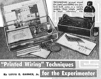
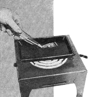
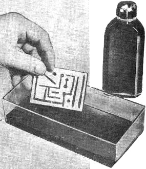
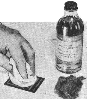
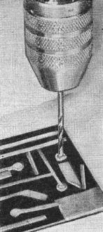
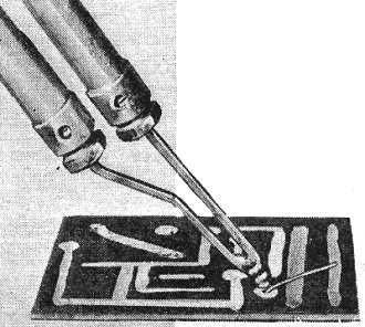
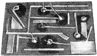
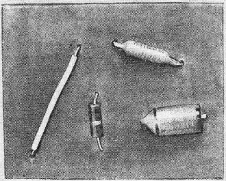
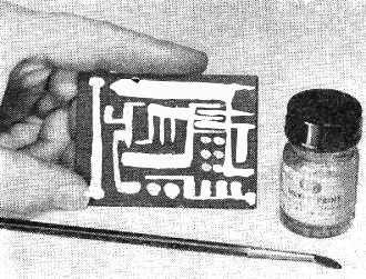
Here is the second of a 2-part article introducing hobbyists to the relatively new technique of printed circuit board (PCB) or, alternately, printed wiring board (PWB) fabrication. Author Louis Garner is from Bell Telephone Labs, which was an early adopter of PWBs. Bell had millions of relay switch and controller circuit boards for routing all the country's telephone calls. I remember a couple times in high school while working as an electrician's helper where we did some wiring inside a phone switching station and saw row upon row of racks of identical panels full of relays. They were clacking busily away in an almost deafening cacophony of non-synchronized noise. It was pretty cool at first, but after an hour or so the novelty wore off and it became annoying. Today, probably all you would hear in a telephone switching station is the sound of cooling fans keeping all the ICs and hard drives within temperature specs. Check out "How to Etch Professional Printed Circuit Boards" Part 1 in the March 1966 Popular Electronics. Part 2 of two-part series presents final steps in making your own etched circuit boards, plus other techniques. Last month we talked about the methods and advantages of substituting printed wiring methods for conventional hand wiring. We also discussed in detail the first four basic steps to follow in making an etched wiring board and assembling a complete circuit: (1) making a layout, (2) preparing the board, (3) transferring layout to board, and (4) applying resist. Step 5 - Etching the Board. A ferric chloride solution (FeCl3) is used for etching the board. This is furnished in either liquid or powdered form in kits. It also may. be purchased at engraving supply houses in liquid form, and from some drug stores and chemical supply houses in powdered or lump form. If you use the etchant from a kit, follow the instructions furnished with it. If you obtain a ferric chloride solution from a photo-engraving supply house, you'll generally find it furnished as "42% Ferric Chloride." This solution is rather thick and may be diluted before use. Add plain water at the ratio of one quart of water to one gallon of solution. If you obtain the ferric chloride in powdered form, dissolve it in a Pyrex glass or an enameled container. Proper ratio is approximately three ounces of ferric chloride to six ounces of water. The dissolving action is exothermic ... that is, heat is evolved as the ferric chloride goes into solution, so don't worry if the solution heats up slightly. Caution: Use care when working with the etchant. It will stain clothing. While not especially dangerous, the ferric chloride solution is "bitey" and may irritate sensitive skin. If possible, wear rubber gloves when working with it. The actual etching is carried out in a small flat tray, similar to those used by photographers. A shallow Pyrex cooking dish makes an excellent tray. Either "hot" or "cold" etching may be employed. The "hot" etching technique is somewhat faster than "cold" etching. With the "hot" etching method, you'll need a small "hot plate" and either a Pyrex dish or tray or an enameled metal tray. If you use the "cold" etching method, a shallow plastic box or tray can serve as the etching container. To etch the circuit board by means of the "hot" method, pour a sufficient amount of the etchant into the tray to cover the circuit board to a depth of about 1/4 to 3/8 of an inch. The actual amount of etchant used is not critical as long as the board is completely covered. If in doubt, always take a larger quantity. Place the tray on the hot plate and turn on the heat. Drop the circuit board gently into the etchant, taking care not to splash the solution. Copper side should be up. Move the board around from time to time during the etching process, using a plastic or glass rod or a pair of plastic tongs. In general, as the temperature of the etchant is raised, up to the boiling point, the faster the etching action. If it is too hot, however, excessive water evaporation will take place, concentrating the solution and slowing the etching process. An "ideal" etching temperature is between 90° and 130° F. After considerable etching using the "hot" method, a little water may be added to the solution to replace the water lost through evaporation. To etch the circuit board by means of the "cold" method, pour about a half-inch of etchant into the tray. A plastic tray may be used. Again, drop the board. gently into the tray, copper side up. Rock the tray slightly during the etching process so that the etchant moves back and forth across the surface of the board. An average circuit board may be etched with the "hot" method in about two to five minutes, depending on the condition of the etchant, the amount of exposed copper, and the actual etching temperature. With the "cold" method, etching time is around ten to twenty minutes. Regardless of the method used, continue the etching process until all exposed copper is removed, leaving only the copper foil protected by the resist. Remove ink resist by rubbing with steel wool, and cleaning with damp soft cloth. Tape resist is simply peeled off. Machining the etched board. When you drill component and eyelet mounting holes in the board, use a solid backing to avoid cracking the phenolic. A drill of the #52 size is generally used, although a slightly larger or smaller drill may be employed sometimes. In the correct soldering technique,. the solder is allowed to flow down to the copper foil. Excessive heat when soldering causes copper foil to separate from phenolic base. When the etching is completed, the etchant may be returned to a tightly sealed storage jar or bottle and the circuit board thoroughly rinsed under clear running water. Allow the board to dry. Step 6 - Cleaning the Board. After thorough rinsing and drying, the resist should be removed from the board, leaving the copper foil "printed" circuit. Ink resist may be removed by rubbing with steel wool, and a final cleaning made using a soft cloth dampened slightly with general-purpose solvent (such as General Cement No. 31-16). Tape resist is simply peeled off. Step 7 - Final Machining. Component mounting and eyelet mounting holes are drilled in the etched board at the points located during Step 3. Normally a size #52 drill is used, but a slightly smaller or larger drill may be employed in some cases. Use a solid backing for the board during drilling to avoid cracking the phenolic. With the drilling completed, mount eyelets (brass or copper) in appropriate holes. Generally, eyelets are mounted wherever connections are likely to be removed and replaced frequently. Where permanent connections are to be made, eyelets are not necessary. Step 8 - Mounting and Soldering. Resistors, capacitors, coils, and similar components are mounted by passing their leads through appropriate holes in the etched circuit board. The customary practice is to mount these components on the "back" (non-etched) side of the board; when mounted in this position, lead tension tends to hold the foil in place instead of pulling it away from the base. Leave the component leads full length. After passing the leads through the holes and pressing the component tightly against the board, the leads are bent slightly to one side, holding the components in, position through natural tension. Circuit crossovers, where necessary, may be made with short lengths of ordinary hookup wire, stripped at both ends. Either a soldering gun or a pencil-type soldering iron with a small (1/8") tip should be used for soldering the connections. Best results can be obtained with a low-melting-point solder such as General Cement #9131 solder and a special printed-circuit soldering flux such as General Cement #12-2 "Print-Kote Soldering Flux." Do not use paste rosin flux nor, under any circumstances, acid-core solder in wiring circuits. The proper soldering technique is to apply a drop of special flux (if used) to the copper foil where the connection is to be made. Then hold the tip of the soldering iron against the lead slightly above - but not touching - the copper foil. Solder is applied to the lead, and allowed to flow down and onto the copper. Remove the iron as soon as the solder flows onto the copper foil. A slightly different technique is to accumulate a drop of solder on the tip of the iron and to hold this against the lead, allowing it to flow down and over the copper foil. Special pains must be taken to complete all soldering as quickly as possible. Excessive heat will result in a separation of the copper foil and phenolic backing. When all leads have been soldered in place, projecting wires may be cut off close to the circuit board, using a pair of diagonal cutters. As a final "touch," the completed circuit may be given one or two coats of silicone resin, either sprayed on from a pressure-type can or applied with a small brush. This insulates and protects the completed circuit and reduces the chances of arcing between adjacent conductors under conditions of high humidity. Either type of silicone resin is available from General Cement as Type 14-6 (spray can) or Type 14-2 (liquid). Short Cuts. The technique of making up etched circuit boards, as described, appears long and tedious. Actually, the work moves much more rapidly, for many of the steps take, at the most, a few minutes. In addition, as skill is gained in making up printed wiring layouts, you'll find you can combine several of the steps. For example, the author seldom makes a circuit layout in advance. Instead, he combines Steps 1, 3 and 4, and, using a tape resist, makes up the layout directly on the copper-clad board. Results obtained by working in this manner are quite satisfactory. "Front" view of completed circuit board, with component leads not yet clipped. Dark stains are caused by liquid flux in soldering the connections. "Back" (non-etched) view of completed board shows parts in position. A piece of hookup wire, stripped at both ends, serves as circuit crossover. "Painted" circuit board made up by applying metallic "Silver Print" on Bakelite base. Eyelets must be used for all connections in painted circuits. More time may be saved by avoiding components requiring large or odd-shaped holes, and by choosing a layout to fit on standard sizes of phenolic board as furnished by the kit manufacturers. Making Painted Circuits. A less popular - but still practical - method of making up a printed wiring board is to "paint" the circuit in place, using a metallic conducting ink on an insulated base. Almost any heat-resistant insulating material will serve as a base as long as it has high insulation resistance and does not tend to absorb moisture. Suitable materials are Bakelite and natural phenolic boards. A suitable metallic paint is General Cement's No. 21-1 "Silver Print." As in the case of the etched circuit board, you make a scale layout first. Then transfer it to the insulating base material. Here the similarity in the two techniques changes. Instead of applying a "resist," the circuit is now "painted" on the board, using a small brush or pen. Since the conductor is a relatively thin layer of metallic deposit, "minimum" width of an individual conductor should be about 1/8" instead of 1/32" ... and, in some cases, it even may be necessary to apply two coats of metallic ink. Drill holes in the board for mounting components, as in the first technique; but since the thin metal deposit will not support a soldered joint, eyelets must be used for all connections. In addition, after you mount the components and solder them in position, it may be necessary to "retouch" around each eyelet to insure a good electrical connection. Of the two techniques for making "printed" wiring boards, the etched circuit board method is preferred for the average home experimenter. It is by far the least critical of the two methods and, although it requires a few more steps, can be carried out with less practice. Advanced Techniques. There are two additional techniques for making up etched circuit boards which have not been discussed. Both of these are simple enough to be practical for use in a home workshop or laboratory, but are better suited for the production of several identical circuit boards than for a "single-shot" circuit. One of these techniques is the "silk-screen" method, in which a silk-screen stencil is first made up and used in applying an ink or paint resist to the copper-clad phenolic. The second technique is the "photographic" process, which involves a light-sensitive copper-clad board. The photographic technique is the one most often used in large-scale commercial work. If there is sufficient interest on the part of Pop'tronics readers in these more advanced techniques, they may be discussed in a future issue ... let us know if you'd like to see such an article.
Posted May 6, 2022 |
|

