The Operational Amplifier: What It Is & How It Works
|
|
Integrated circuit (IC) designers have been striving to make the "ideal" operational amplifier (opamp) ever since the device type was first conceived. An ideal opamp has a certain set of well-defined properties that permit it be used in circuits defined by neat mathematical equations without the need for compensating or limiting terms. An example of compensation might be having an input impedance of something other than infinite ohms that causes a voltage division effect on the input voltage, and a limitation would be a gain-bandwidth product that prevents it from being used in high frequency applications. Opamps appeared in electronics before semiconductors came onto the scene, and a couple companies attempted to market prepackaged vacuum tube opamps that plugged into a standard octal kind of socket (see Part 2 of this series). EE120 at the University of Vermont (my alma mater, class of 1989) introduced me to operational amplifier theory, and I remember being amazed at the design of the μA741 opamp used in the textbook. The "741" is quite crude by today's standards, but it still represents the basics of opamp implementation. I was so impressed with the device that after graduation and working at my first job as an electrical engineer at General Electric in Utica, New York, the three-number sequence was used as the combination on my newly acquired briefcase (we wore suits and carried briefcases back in the day). This Versatile Linear IC Opens up Many New Areas for the Serious Experimenter
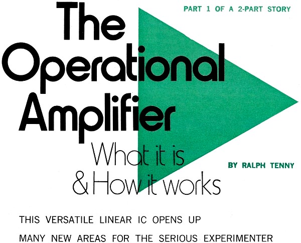
By Ralph Tenny The operational amplifier (usually shortened to op amp) is actually nothing more than a de coupled amplifier with very high gain and with external components connected to it to control its response characteristics. Though there was nothing new about the circuit, the term operational amplifier gained recognition in the early days of electronic computation when op amps were first used to perform certain mathematical operations. Today's op amp (usually referring to an integrated circuit device) approaches in performance the elusive "perfect amplifier" which, if it existed, would have the following characteristics: 1. Infinite gain; a very small change in input should produce an infinite change in output. 2. Zero output for zero input. 3. Infinite input impedance; no power consumed from the driving source. 4. Zero output impedance; output voltage should remain the same even if load resistance drops to zero. 5. Infinite bandwidth; zero rise time. 6. Insensitivity to either power supply or temperature variations. Although such a perfect amplifier has not yet been developed, modern semiconductor technology has produced an op amp whose characteristics come quite close to the perfect case.
Fig. 1 - The basic arrangement of a typical op amp. Such a circuit could contain up to a couple of dozen transistors and associated resistors, all on a very tiny silicon chip.
Fig. 2 - A perfect amplifier would have these characteristics. Although still a dream, such a circuit may not be too far in the future.
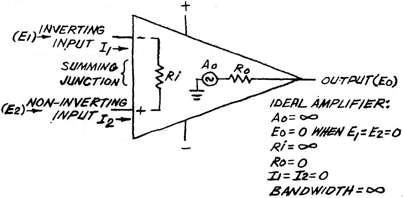
Fig. 3 - This basic differential amplifier is found in op amps. The biasing of Q3 determines the amount of current flowing in Q1 and Q2. A differential pair produces a far greater output swing than a single transistor.
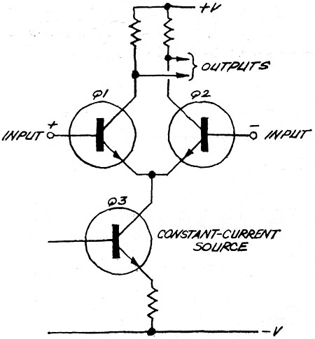
Fig. 4 - The output of an op amp when a positive step is applied to the inverting and non-inverting inputs.
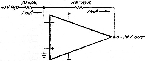
Fig. 5 - Resistor R2 is the feedback resistor while R1 is an isolator and represents circuit input resistance.
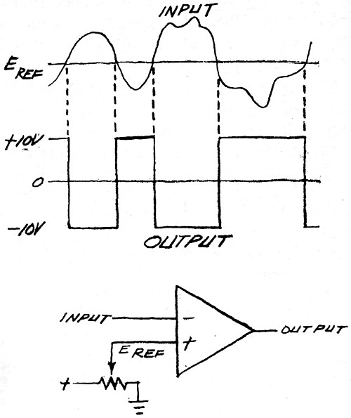
Fig. 6 - When input exceeds reference, the output is negative, and vice versa.
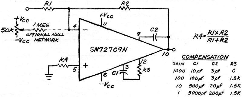
Fig. 7 - Capacitors C1 and C2, and resistor R3 form the op amp compensation. Nulling can be via optional resistor network.
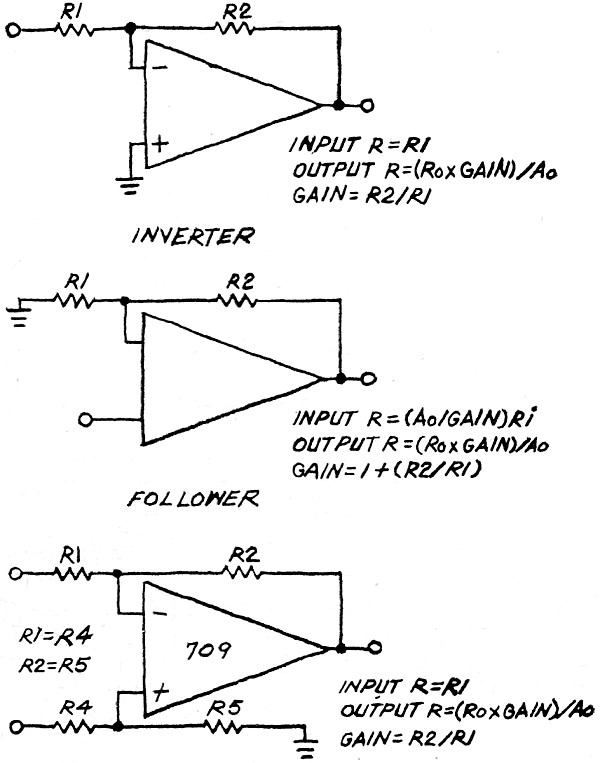
Fig. 8 - Three typical op amp uses. Inverter (A), follower (B), and difference amplifier (C). Also shown are the basic equations for input, output, and gain. The difference amplifier output is proportional to the voltage difference between the two signal inputs.
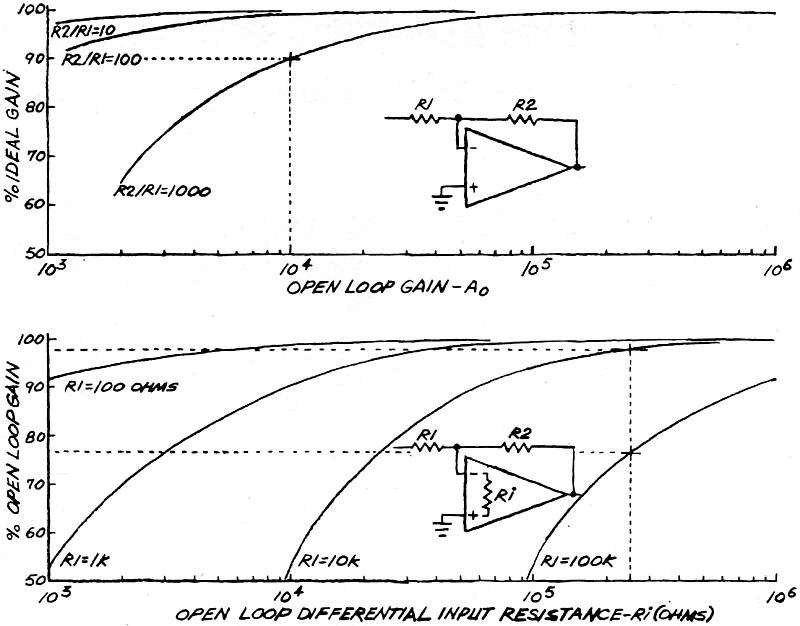
Fig. 9 - Open loop gain and differential input resistance vs performance.
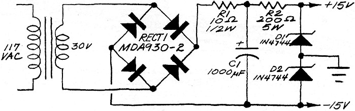
Fig. 10 - Simple power supply for op amp experiments.
Fig. 11 - Battery operated power supply delivers two polarity outputs. What's in an Op Amp? A typical op amp consists of three basic parts as shown in Fig. 1: a high-impedance differential amplifier that has low drift and wide bandwidth; a high-gain stage; and an output stage that isolates the gain stage from the external load and provides the actual power output. The conventional symbol for an op amp, together with the characteristics of a perfect amplifier are shown in Fig. 2. Note that both polarities of the supply voltage are used (with the common grounded). This is necessary for the op amp to be able to deliver both positive and negative (with respect to ground) signals at the output. The schematic of a basic differential amplifier is shown in Fig. 3. The currents to the emitter-coupled transistors (Q1 and Q2) are supplied by the constant-current source (Q3). The characteristics of the differential pair and the associated resistors are closely matched in the manufacturing process, If the two input voltages are either zero or are similar in level and polarity, the amplifier is balanced because the collector currents are equal. Therefore, a zero voltage difference exists between the two collectors. The sum of the emitter currents is always equal to the current supplied by the constant-current source so that, if one transistor draws more current, the other must take less. Thus if the input to one transistor causes it to draw more current, the current in the other decreases and the voltage difference between the two collectors changes in a differential manner. The differential swing is greater than the simple variation that can be obtained from only one transistor. To further understand the operation of the differential amplifier, consider the diagrams in Fig. 4. In A, a positive-going signal applied to the minus input produces a negative-going output. Thus the configuration at A is called an inverter and the minus input is called the inverting input. If the same signal is applied to the positive (non-inverting) input, the output is positive-going and the configuration is called a follower. Because no feedback is used in Fig. 4, the amplifiers are operating "open loop" and a small input produces a large output. Actually, operational amplifiers are usually used with some form of feedback (closed loop) as shown in Fig. 5. In this inverter arrangement, feedback resistor R2 is connected from the output back to the inverting input to produce a signal which works against the input to reduce its effect. Resistor R1 isolates the inverting input from the signal source and represents the circuit's input resistance. The non-inverting input is grounded in this case. Assume that a 1-volt signal is applied to R1. Due to the high input impedance of the op amp, essentially no current will flow into the input terminal (also called the summing junction), and there is a zero voltage drop between the two input terminals. The summing junction remains at zero potential. Since R1 is 1000 ohms, the 1-volt input signal creates a current of 1 mA through R1 and it flows also through R2 to the output terminal. However, 1 mA of current through the 10,000-ohm resistor creates a voltage drop of 10 volts so the output terminal must go to -10 volts. Thus the configuration is a gain-of-10 inverter. Frequency sensitive networks can be used with op amps to create oscillators and frequency selective amplifiers. With a capacitor in the feedback loop, the op amp acts as an integrator; and with a capacitor in the input, a differentiator is formed. Feedback is not necessary in some op amp circuits. For example, if one input is connected to a reference voltage and the other to a varying input signal (see Fig. 6), the open-loop amplifier will respond to the potential difference between the two inputs. Due to the high gain, the output level will swing widely (almost equal to the power supply voltages) as the varying voltage equals and exceeds the reference voltage. Note the input-output waveforms shown in Fig. 6. When the input signal is less than the reference, the op amp output is highly positive, and vice versa. If the two inputs were reversed, the phase relationships would also be reversed. Other op amp circuits can be used as multi-signal summers, adders, or subtraction circuits. The second part of this article will illustrate a number of practical examples. Compensation. Because high-gain op amps are usually used in a feedback mode, the feedback must be controlled to assure that the circuit is stable with frequency and will not oscillate if the input-output phase difference changes drastically. When no phase compensation is furnished, the gain of the feedback signal may be greater than unity when the phase angle approaches 180°. In this case, feedback that is negative at low frequencies, becomes positive at higher frequencies and unwanted oscillation may result. To overcome this tendency toward un-wanted oscillation, the frequency response and phase-shift characteristics of the op amp must be compensated - that is, outboard passive components (usually resistors and capacitors) are used to tailor the frequency response and phase-shift characteristics. One form of compensation uses a resistor and capacitor in series. In this case the amount of feedback increases as the frequency goes up and the reactance of the capacitor goes down; but the upper limit is determined by the resistor value which remains constant at the high frequencies. Another popular form of compensation is called output limiting and can take the form of a low-value capacitor connected from the output back to the input. This output compensation is used to supplement the other compensation. The type of compensation used in any case is unique for the type of op amp and the application. Sometimes compensation is obtained by bypassing the op amp to ground. If an op amp requires compensation, suitable terminals are provided on the package. There are some types that require no compensation and are so identified in the manufacturer's specifications. A typical circuit with compensation is shown in Fig. 7. This circuit also has a null network which balances out the effect of offset voltage and current. This will be discussed later in more detail. Each circuit using an op amp has certain closed-loop characteristics that must be taken into account by the circuit designer. For example, Fig. 8 shows the basic characteristics of a follower, an inverter, and a difference amplifier whose output is proportional to the difference between the two inputs. Performance Limitations. Op amps have performance limitations - as do all electronic components. These limitations are given in the specification sheets but for most purposes, the critical performance specs are power output, open-loop characteristics, bandwidth, input limitations, offset voltage, and offset current. The most important specification is usually power output. The popular 709 IC op amp will develop ±10 volts at 5 mA output, using a bipolar 15-volt power supply. Note that the 5 mA is the total output current, including that used by the feedback network. The effects of open loop gain and differential input resistance on final circuit performance are given in Fig. 9. To use the open loop gain graph, draw a vertical line at the open loop gain of the op amp being used. Where this line cuts the curve determined by the resistance values (R2/R1), read the percentage of ideal gain on the vertical axis. In the example in Fig. 9, the open loop gain was 10,000, R2/R1 was 1000 and the percentage was 90%, meaning that the gain is actually 900 (90% of R2/R1). The lower graph of Fig. 9 shows the effect of the external resistors on open loop gain as a function of the open loop input resistance. It also demonstrates that the open loop input resistance should be as high as possible. For example, a typical 709 has an input resistance of 250,000 ohms. Draw a vertical line from this point on the horizontal axis. If R1 is 100,000 ohms, the open loop gain would then be 77% of normal. In this case the specified open loop gain is 50,000, so the actual gain would be 38,000. This is the figure to be used in determining ideal gain from the upper graph in Fig. 9. For the same amplifier, if R1 is reduced to 10,000 ohms, the open loop gain would be 95% of the specified 50,000. For R1 = 1000 ohms or less, the effect of open loop gain would be minimal. Of course, R1 determines the input resistance so this factor must be taken into consideration. Bandwidth and Slew Rate. Suppose a high-frequency, high-amplitude signal is fed into the op amp. Because the various elements within the op amp have some capacitor characteristics (mainly semiconductor junctions and strays due to proximity of conducting paths) a finite amount of time will be required to charge and discharge them. This prevents the output voltage from following the input signal instantaneously. Thus, these internal capacitances limit the rate at which the output voltage can change or slew. The maximum time rate of change of the output is identified as the slew rate and is specified as volts per microsecond. The slew rate of a feedback amplifier depends on a number of factors, including the value of the closed loop gain. Bandwidth and slew rate are related in that slew rate limits the bandwidth. The latter is usually expressed as a large signal bandwidth or the highest frequency at which the amplifier will develop its rated output without distortion. A particular amplifier is capable of having a higher frequency response with a smaller output. Offset Error. Even though extreme care is used in the fabrication of an op amp, a very slight mismatch may still occur between the internal components. The result of this mismatch prevents the amplifier from having a zero output for a zero input. This, of course, may be a problem when using the op amp in a dc circuit. Compensation for this offset voltage is made by using a nulling network such as that shown in Fig. 7, in which the nulling potentiometer is adjusted for zero output with zero input. Common-Mode Error. Because it is very difficult to create a perfectly balanced system, the signal present at one input of a differential pair may affect the signal on the other input. The result is called common-mode error and it is smallest when the specification called "common-mode rejection ratio" is the highest. Power Supply Considerations. Changes in the power supply of an op amp circuit often change the open loop gain, the common-mode input limits, and the input bias current. For example, the open loop gain of a typical 709 doubles when the power supply is changed from ±10 to ±15 volts. Input voltage limits change in proportion to the supply voltage and the bias current increases about 10% for a 50% increase in the supply voltage. This sensitivity to power supply voltage seems to rule out batteries as a source but this need not be true. Circuits of moderate impedance having gains of 100 or less will not degrade appreciably if batteries with high current capacity are used and they are changed frequently. Mercury and rechargeable nickel-cadmium types have "flat" discharge curves and give good performance for a premium price. If battery power is a necessity, some manufacturers make discrete amplifiers for use with unregulated supplies. Power supplies regulated by Zener diodes furnish regulation close enough for most op amp applications. A typical supply of this type is shown in Fig. 10. Note that neither side of the filter capacitor is grounded since the supply develops both positive and negative voltages. The triangular ground symbol between the two diodes is an "instrumentation ground" and indicates that all ground connections within the system should be connected together but grounded to the chassis at one point only. This minimizes circulating ground currents. In extreme cases, the input connectors are also isolated from the metallic ground and connected to the instrumentation ground only. The circuit of a single-battery, Zener-controlled supply is shown in Fig. 11. The emitter resistor should be chosen so that the current through the Zener diodes is about 50% above that required for the amplifier and associated load. Critical op amp circuits require extremely close regulation - similar to that provided by a high-quality supply that uses one of the commercially available IC voltage regulators. No matter what type of power supply you use, all op amp manufacturers suggest the use of a bypass capacitor close to the amplifier on the power supply leads. In fact this is mandatory if power supply leads are long. The recommended capacitor size is about 0.1 μF. [Part 2, on applications, will appear in the September issue.-Ed.]
Posted July 9, 2019 |
|