The MOSFET
|
|
The metal-oxide-semiconductor field-effect transistor (MOSFET) was patented in its present form by Bell Labs in 1959, following the original patent by inventor Julius Edgar Lilienfeld, in 1925. It had only been on the open market for designers to use for a bit over a decade when this article appeared in Popular Electronics. Adolph A. Mangieri wrote a number of articles for the magazine in the early 1970s introducing readers to the many new types of semiconductor devices coming out of research laboratories and into the commercial marketplace; e.g., "Understanding the Junction Field Effect Transistor." MOSFET's are nowadays the primary building blocks of digital circuitry due to their low power operation compared to junction transistors. The MOSFET - How it works and some practical applications By Adolph A. Mangieri
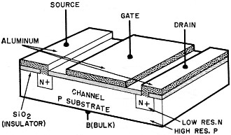
Fig. 1 - How n-channel MOSFET is fabricated. Applications for and usage of the insulated gate field effect transistor (MOSFET, IGFET, or MOS transistor) are growing by leaps and bounds. Problems of high cost and frequency limitations which were initially encountered have been overcome by improvements in MOS technology and the IGFET is now competitive in price with other transistors both as discrete units and as parts of integrated circuits. Micropower logic is made possible by complementary MOS circuitry with switching speeds suitable for many applications. Particularly adaptable to MSI and LSI digital circuits, the MOS transistor, long in the background, in now the focal point of accelerated research and development. Fabrication and Operation. An n-channel MOS transistor is fabricated on one side of a silicon p substrate by the planar process. Two elongated strips of heavily doped, low resistivity n regions are diffused into the substrate to form the drain and source (Fig. 1). A very thin layer of insulating silicon dioxide (special glass) is formed over the entire surface. A portion of the insulator is then etched off to expose the source and drain elements. Next, an insulated gate electrode is formed over the channel and connections are made to source and drain by aluminum metallization. There are no rectifying junctions.
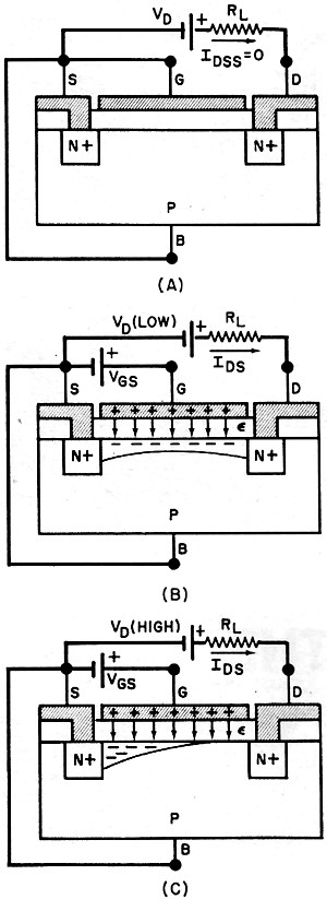
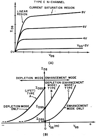
Fig. 2 - Diagrams show how current in FET varies with changes in drain and gate voltage. As shown in Fig. 2A, with drain-source voltage applied and gate voltage at zero, the pn junction at the drain is reverse biased. The drain current is near zero. When the gate voltage is increased from zero, the electric field within the oxide and semiconductor increases. When the gate voltage exceeds a threshold, the electric field induces free electrons in a very thin layer at the top of the channel. Current may now flow from drain to source by means of free electrons or by n-type conductivity. In effect, the p channel has been inverted to n conductivity by the electric field. Although it has a p channel, the transistor is termed an enhancement mode n-channel IGFET or a type C FET. Operation at a low drain voltage (Fig. 2B) produces a uniform inversion layer along the channel. This is operation in the linear region indicated on the static characteristics in Fig. 3A. In the linear region, the MOS transistor simulates a resistor whose value depends on the gate voltage. At higher drain voltages, the inversion layer is pinched off at or near the drain end (Fig. 2C). Channel current becomes dependent on gate voltage and nearly independent of drain-source voltage. This is operation in the current saturation region along the horizontal portions of the characteristics. This is the operation normally used for MOS amplifiers and constant-current sources. The MOS transistor is then a square-law device showing curvature of the input-output transfer characteristics (Fig. 3B). This is also suggested by the unequal spacings of the static characteristics. Junction field effect transistors (type A FET's) are similarly nonlinear. A second type of MOSFET operates in the enhancement-depletion mode (type B FET). An n-channel depletion-mode MOS is similar to the enhancement device but also has an n region diffused into the surface of the channel. The n region bridges the source and drain and introduces a built-in layer of free electrons. As a result, the zero gate voltage drain current IDSS is intermediate (Fig. 3B). Unlike type A and type C FET's, the type B can be operated with plus or minus gate polarity. The p-channel MOSFET is similar in construction and operation but uses n substrates and p source and drain regions. The polarities of operating voltages are reversed. The very thin gate oxide layer is quite susceptible to puncture by static electricity. For this reason, MOSFET's have a shorting ring or wire on the leads. The shorting device is removed only after the transistor is installed. Some discrete and many IC MOS devices include a built-in diode to protect the gate. Specifications for the MOSFET include gate leakage current (IGSS) which is in the nanoampere or picoampere range. Gate leakage resistance is extremely high - millions of megohms. Forward transconductance (Yfs) is usually between 500 and 15,000 micromhos. The frequency response of the MOS transistor is limited primarily by gate capacitance. Small-signal input capacitance is about 3 to 15 picofarads. The frequency response of available types extends to 400 MHz. Recently developed devices having very short channel lengths and lower parasitic capacitances have extended the usable frequency range up to 10 GHz.
Fig. 3 - (A) Static characteristics of type C FET; (B) transfer characteristics of 3 types.
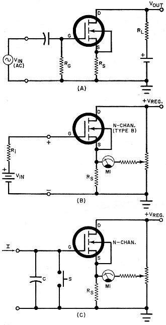
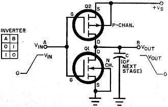
Fig. 4 - Some typical MOSFET applications. Applications. Almost any application for the junction FET can also be handled by the MOS transistor. These include low-level audio and r-f amplifiers, oscillators, mixers, modulators, switching circuits, choppers, etc. A high input impedance audio pre-amplifier as shown in Fig. 4A uses an n-channel depletion mode MOS. Source resistor R, provides gate bias voltage and negative feedback for improved linearity and stability. Unique applications of the MOS transistor rely on the fully insulated gate and high input resistance. The "infinite" impedance dc voltmeter shown in Fig. 4B is nonloading. The addition of a high-resistance input voltage divider and gate protection diode makes a practical voltmeter with input impedance from 10 to 100 megohms per volt. By connecting a low leakage capacitor across the input, the voltmeter becomes a dc current integrator, a "read and hold" voltmeter, or an electrometer (Fig. 4C). The latter measures minute dc currents by accumulating a charge on the capacitor over a known time interval. The indication on the meter is proportional to the accumulated charge, allowing determination of the current charging the capacitor. An electrometer also serves as an electroscope to detect ionization levels of air or gases. The switch on the input allows resetting of the meter by discharging the capacitor. A familiar application of this circuit is the photographer's electronic flash meter. When a suitable resistor is placed across the gate input in Fig. 4B, the circuit becomes a sensitive current meter. Full-scale indications of several nanoamperes can be obtained by using a 100-megohm resistor as a current shunt. Currents in the pico-ampere range (and lower) are measured using more complicated circuits, selected transistors, and highly insulated construction. A very important application of the MOS transistor is in digital integrated circuits. MOS logic has high noise immunity because the gate voltage swings for turn-on are in the "volts" range. Of even greater importance is the remarkable reduction in power consumption afforded by complementary MOS micropower logic circuits, which utilize p- and n-channel transistors in a complementary circuit. The power consumption of the circuit is near zero on standby and very low when the circuit is switched. A basic circuit in micropower logic is the complementary inverter shown in Fig. 5. Channels of the n-channel transistor and its p-channel complement are connected in parallel. Both are enhancement mode transistors, with Q1 requiring a positive gate voltage for turn on and Q2 a negative gate voltage. A logic one signal raises the input to +Vs and a logic zero returns the gates to ground. If Vin is zero, Q1 is off because VGS of Q1 is zero; but VGS of Q2 is minus, so it is on. Capacitor C (gates of following stages) charges up to +Vs and current flow drops to IDSS of Q1 (in the picoampere range). The output is high at logic one. When Vin is raised to Vs, Q2 turns off and Q1 turns on and the capacitor discharges rapidly to zero. At present, complementary MOS switching speeds are under 10 MHz; recent developments assure higher speeds.
Fig. 5 - Low-power complementary inverter.
Posted March 22, 2018 |
|