What Are All Those Extra Components For?
|
|
Maybe what piqued my interest in electronics enough during my teenage years to eventually enter into the field as a lifelong vocation was wondering what the heck all those components were doing that were sprinkled around circuit boards and inside product housings. The circuits I was building at the time were typical beginning hobbyist types with just enough capacitors, resistors, inductors, diodes, etc., to make the lamps blink properly or to pick up a strong local AM radio station. Even in undergraduate college circuit design classes we rarely went beyond noise bypass capacitors on ICs or counter-EMF-snubbing diodes across solenoid coils. Having already been in the electronics world for many years before college, I knew there was much more involved in producing reliable, trouble-free circuits that worked well in a range of environments, and therefore was surprised to find that those aspects of product design were left to personal study and on-the-job-training after graduation. What Are All Those Extra Components For
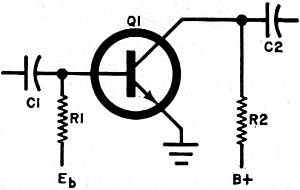
By Jim Huffman Students of electronics are often confused by how much more complex a practical circuit often turns out to be when it is compared to the classical circuit from which it was derived. Under such circumstances, the most often asked question is: "What are all those extra components for?" Let us first assume that, in practical manufacturer circuits, every component used is there for very good reasons, specifically to obtain proper operation from the circuit. It then remains only to understand the function of each component and how it aids in the operation of the circuit. If proper understanding of classical and typical circuits is achieved, little difficulty should be encountered in analyzing the operation of practical circuits. Knowing the function and/or mode of operation of the circuit can provide the key to why a particular component or components are used in any given circuit. Classical vs. Practical. In Fig. 1 is shown a typical common-emitter amplifier stage. The thing to remember with "classical" circuits used in textbook theory - and this circuit is such an example - is that an absolute minimum of components is ever shown.
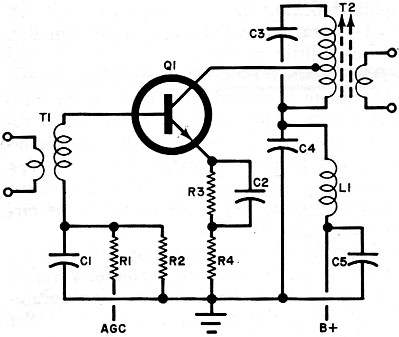
Fig. 1 - Classical common-emitter circuit with basic, essential components. Transistor Q1 serves as a current amplifier. A small current applied to the base initiates and controls a much larger current flow in the collector circuit. The current applied through biasing resistor R1 to the base of Q1 is supplied by Eb. In the absence of an input signal at C1, the bias current is a function of the voltage level of Eb and the resistance value of R1. Capacitors C1 and C2 couple the signal into and out of the circuit, respectively, while blocking dc to prevent upset of the bias on this stage and the next. Resistor R2 is the collector load that allows the output signal to be developed between the collector of Q1 and ground. While the functions of the components in Fig. 1 are easy to see, a different frame of reference must be used when you are confronted with the practical circuit in Fig. 2. The key here is that this is an r-f amplifier stage of a type commonly used in radio receivers. Once this is known, it is fairly easy to explain the existence of L1, T1, and T2 as having something to do with providing proper operation at radio frequencies. But what about the extra capacitors and resistors? By using some logic, you can see that the R1/R2 combination performs essentially the same function as that performed by R1 in Fig. 1. Note also that R2 is grounded at one end and that R1 is a special input for an automatic gain control (agc) signal. The agc is a voltage, the value of which depends on the level of the input signal at T1. When the agc voltage increases, bias on Q1 increases and stage gain decreases. Consequently, the agc voltage is similar to biasing voltage Eb in the classical circuit. Capacitor C1 in Fig. 2 functions in a manner similar to C1 in Fig. 1. That is, it blocks dc bias voltages. Also, it places one side of T1's secondary at r-f ground, allowing the full output from the transformer to be impressed on the base of Q1. If C1 were not in the Fig. 2 circuit, R1 and R2 would reduce signal level and diminish stage gain.
Fig. 2 - Practical r-f amplifier has much more complexity when compared to the circuit from which it was derived. Although it is more complex, the output section of Fig. 2 corresponds in performance to the two-component output section of Fig. 1. Transformer T2 provides dc isolation and matches the output impedance of Q1 to the input impedance of the next stage. So, the primary of T2 functions as the collector load for Q1. The tap on the primary of T2 is for matching the low output impedance of Q1 to the higher impedance of the transformer's primary. This is done so that a practical value for C3 (which forms a tuned circuit with the primary of T2) can be selected to provide a reasonable Q for the tuned circuit. Capacitor C4 is used to connect the lower end of T2' s primary to r-f ground and block dc. Coil L1 has a large reactance to r-f and "chokes" any r-f that might get past C4 into the power supply. A large value of capacitance for C5 insures against variations in the output signal caused by agc action. These are low-frequency variations which, if they got into sensitive stages via the power supply leads, can really mess up the sound from the receiver. There is one more circuit to call attention to-the emitter circuit of Q1. Here we see components that do not even exist in the classical circuit in which the emitter goes directly to ground. The differences in bias arrangements account for the extra components in the practical circuit. The classical circuit employs a separate biasing supply (Eb), but our practical circuit is self-biased. Resistors R3 and R4 should be treated as a single emitter resistor. Capacitor C2 is there to by-pass r-f around R3 so that it does not affect the circuit during biasing. Resistor R4 carries both dc and r-f. This is done to introduce negative feedback to the r-f signal. Some of the current flowing between the emitter and collector of Q1 causes a voltage to be dropped across R4. This drop is wasted; so the presence of R4 in the circuit decreases stage gain, a form of negative feedback. The obvious reason for R4 being where it is, then, is to provide the circuit with a measure of overload protection. Enough gain can be obtained from later stages to cancel the losses introduced by R4.
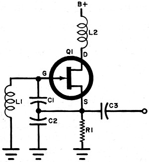
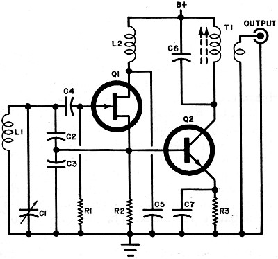
Fig. 3 - Typical textbook VFO circuit has little practical use as it stands. Rules of the Thumb. From the foregoing, we can establish some "rules of the thumb" that can help us in analyzing any circuit and clear up doubts about extra components. The first of these is that coupling capacitors are usually in series with the signal path. Also, in connection with capacitors, bypass capacitors route signals around a component or circuit. Next, coils without parallel capacitors are usually just chokes. Transformers represent output loads and perform the dc blocking function of capacitors. There are other rules you can add to this list as you become more proficient in analyzing circuits. Let us take one more example of classical-versus-practical circuits. In Fig. 3, you see the classical representation of a FET variable-frequency oscillator (VFO). It is fairly easy to understand the function of each component in this circuit. The drain and gate signals of FET Q1 are 180° out of phase with each other. Coil L1 is center-tapped by the C1/C2 arrangement. Since L1 is tapped, the signal from the drain of Q1 undergoes another inversion in the coil, and actual feedback to the gate of Q1 is in-phase with the output signal. The in-phase condition causes the output to reinforce the input and oscillation occurs at a frequency determined by the values of C1, C2, and L1. Coil L2 serves as the drain load for Q1 and its high reactance prevents the output signal from the FET from feeding into the power supply. Resistor R1 provides source bias. Capacitor C3 is a signal coupler that passes the output signal into the next stage while blocking dc. The practical VFO circuit shown in Fig. 4 bears little resemblance to the classical circuit. Probably the most confusing part of this circuit is the addition of an extra transistor stage. Obviously, to obtain good results, the Fig. 3 circuit needs some isolation; not to mention extra drive. For this reason, the buffer stage (Q2 and its associated components) were added to the circuit in Fig. 4.
Fig. 4 - Practical VFO uses an extra stage (Q2) for buffering and extra components to give stability. Now, let us analyze the rest of the circuit as we did in the previous example. Variable capacitor C1 provides a means for accurately adjusting the output frequency of the oscillator. Resistor R1 connects the gate to the source of Q1, providing both bias and a means for developing a signal voltage. Capacitor C4 and resistor R1 keep dc out of the tuned circuit, thus aiding in operational stability. Capacitor C5 serves as a bypass that routes the signal on the drain of Q1 to ground. Note that Q1 is set up in a common-drain configuration. The gate is used for an input and the source for an output. Thinking of the oscillator in this light, you can see that the ground connection is the same as the connection in the classical circuit that led from the drain to the gate. Alternatively, C5 can be viewed as a coupler in series with the signal flow. One more point on the circuit. There is no coupling capacitor between the source of Q1 and the base of Q2. In this case, Q2 obtains bias from Q1 and R2 with both components serving as the bias resistance. Hence Q1 and R1 in Fig. 4 correspond to R1 and R2 in Fig. 2. As we have demonstrated, classical or typical circuits are not always - and, in fact, rarely are - the same as the practical working circuits. But if you work on the assumption that every extra component used is there to aid in circuit performance in some way and you apply a few rules of thumb, you will be able to interpret a circuit's diagram quickly and be better prepared when it comes to troubleshooting and repair.
Posted January 22, 2024 |
|

 They have practical reasons for being in the
circuit.
They have practical reasons for being in the
circuit.