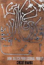
How to Etch Professional Printed Circuit Boards
|
|
How to Etch Professional Printed Circuit Boards Be As Good As The Experts By James A. Gupton Jr.
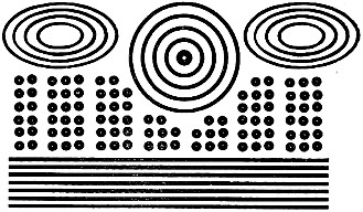
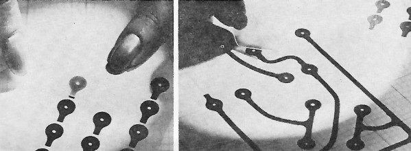
Fig. 1 - Once the basic layout is made, you can use tape resist transfer sheets like these to give your circuit board a really professional appearance.
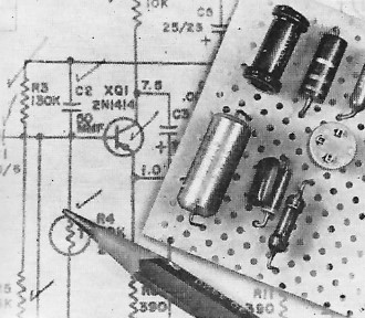
Fig. 2 - Carefully redraw the schematic for best layout of components, using the actual parts to determine minimum spread between component leads.
Fig. 3 - Mock-up of printed circuit board showing preliminary parts layout. Terminals are interconnected in accordance with circuit schematic diagram.
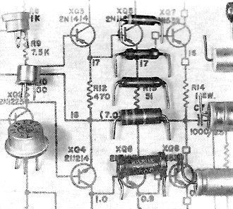
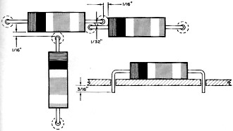
Fig. 4 - Shown here is the minimum allowable spacing between adjacent PC board components and leads. The Hobbyist who has totally escaped the era of microminiaturization must live a sheltered life, indeed. For, with the expanded use of transistorized circuits - not to mention monolithic integrated circuits - in everything from toys to television sets, no up-to-date experimenter can stand idly by in the presence of this great technological revolution. Much of the credit for this rapid change in manufacturing technique belongs to the space-age scientists whose constant demand for more complex instrumentation in the limited space aboard orbiting satellites has revolutionized the electronics industry. Yet, at the heart of every miniaturized circuit stands the "printed circuit," which came into being more than a decade ago. Printed Circuit Techniques. The general term "printed circuit," or "printed wiring," as it is sometimes called, refers to a laminated board with an insulating base. The base material is usually a phenolic board to which a layer of metal foil is bonded. The foil may be on either one or both sides of the board. Printed circuits offer many advantages to the experimenter, hobbyist, and engineer. With relatively little practice on the part of the builder, a complete printed circuit can be produced in less time than is required to make a wired circuit, and with a substantial reduction in space requirements. They can be produced by many different processes including etching, stamping, embossing, and plating. Of the various techniques that can be used, the etching process is by far the least expensive and most popular method. It is also the simplest and most adaptable to the needs of the home builder. The basic materials you will need are described below. Making an Etched Circuit. An etched circuit is made by masking certain portions of a copper-clad laminate circuit board with an etch resistant ink or tape strips (called "resist") to correspond to specific circuit wiring. Then the entire circuit board is immersed in an etching solution which etches away all unmasked copper, without affecting the phenolic board. After the resist is cleaned off the etched copper, the printed circuit is ready for use. As a beginner, you'll probably find it both convenient and economical to start with one of the many printed circuit kits which you can buy from most electronic equipment supply houses. The kits contain a variety of materials and parts including etching solution, a glass or plastic tray (or bag) in which to do your etching, printed circuit sockets, liquid or tape resist materials, and an assortment of copper-clad circuit boards. If you plan to do a lot of etching, you'll probably be better off buying just the right material in the amounts needed for a particular job. Printed Circuit Boards. Most parts distributors carry a large assortment of printed circuit boards. These are of the copper-clad type which provide high conductivity and good solderability. For special applications, other metal foils such as silver or aluminum can be used; these are non-standard materials, however. Copper thicknesses vary from 0.0007 to 0.0094 inch. The circuit board base is usually made from Bakelite, epoxy, silicon, Teflon, fiberglass, or paper-base phenolic material that has been impregnated or coated with a thermo-setting phenolic resin and pressed into a hard solid sheet. The phenolic board is by far the most widely used. If you ask your parts distributor for Vectorbord, you are sure to get the right thing. The sheets are available in thicknesses ranging from 1/64 to 1/4 inch. For most applications, the 1/16"-thick boards (approximately 2 mils) are ideal. The electrical properties of paper-base laminates are set by the National Electrical Manufacturers Association (NEMA), and consist of the following grades: X, XX, and XXX. The letter "P" after the grade designations, as in XXXP, denotes that the material has good punching qualities. The best electrical properties are found in Grade XXXP, while Grade X has the poorest, and costs less. Etchant Resists. The ink, tape strip, or other materials that are used to mark those areas of the copper laminate that make up the printed circuit, is referred to simply as resist. There are many different types of resists on the market; paraffin wax, special types of ink, resists in tubes with ball tips for writing on the copper, and press-on adhesive tape, are among numerous types that can be used.
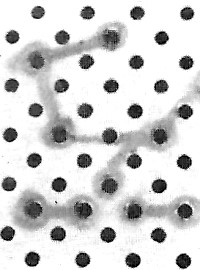
Fig. 5 - Reverse side of mock-up circuit board with lines drawn to connect terminal leads. PC board follows this pattern. The recent appearance of a wide assortment of etch-resist transfer sheets with straight lines, circles, ellipses, and dozens of pads with different diameters definitely add a professional touch and tend to obsolete all other types. The designs of one manufacturer, Emi-Tron Associates (North Hollywood, Calif.) are shown in Fig. 1. Etchant Solution. For the etchant solution, you have a choice of acids, oxidizers, or corrosive alkali. Of all these, ferric chloride is the most popular. Another widely used etchant is ammonium persulfate, the main advantage of which is that it does not contaminate the insulating phenolic board during the etching process. Acids are the least desirable since they produce an exothermic reaction when diluted. However, if you do want to use an acid, the cardinal point to remember is that you must add the acid to water when diluting a concentrated solution. Never add water to the acid because the heat resulting from the reaction will cause the water to boil and might spatter the acid. If you use ferric chloride powder, dissolve one pound of the powder into one pint of hot tap water. Slowly pour the ferric chloride into the water, allowing the solution to cool off when it becomes hot before adding additional ferric chloride. If you are using a concentrated solution of ferric chloride, you must first pour the solution into a mixing bowl, and then add water according to the directions that come with the package. When completely dissolved, the ferric chloride will have a dark reddish brown color. A word of caution: watch out for ferric chloride stains on your clothes and hands. Making a Layout. First you must plan your circuit board layout on paper - preferably on graph paper. This means you must study the schematic diagram carefully and then try to layout the board to suit the circuit. The trick is to redraw the circuit in such a way that the "wires" don't cross each other, and this is not always an easy task. The characteristic patterns you see on a printed circuit board are largely due to this effort.
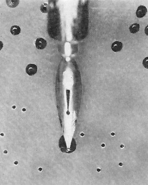
Fig. 6 - Use a pen or other applicator to put on liquid resist. After all drilled holes are circled, draw lines to connect them following your sketch.
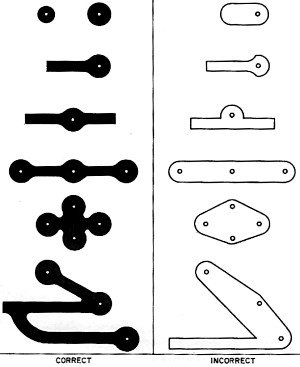
Fig. 7 - As you work, be sure that paths are properly terminated as shown here. Incorrect terminations may result in poor etching and circuit arcing.
Fig. 8 - Resist transfer sheets being applied. Rub on over desired area and peel back sheet leaving resist on surface. Where conductors must cross, as they sometimes will, select a point where a resistor, coil, or other circuit component intersect, and then let that component bridge the gap. If you find you can weave all your circuit paths to keep conductors from being boxed in when they are to continue to another point on the circuit board, you just know you are working like a pro. If - after you have exhausted all your efforts and skills - you find you are still fenced in, terminate the lead near the crossing point and continue on the other side of the line without touching the conductor being crossed. Later you can drill a hole at each end where the interrupted lead should meet, and then bridge the gap with a jumper wire while you are assembling the circuit. In general, component and wiring leads can be soldered directly to the copper foil for permanent connections. But if the leads may have to be removed often, plan on using copper or brass eyelets at such points. Preparing the Board. In addition to the copper-clad board which is going to be etched, secure a piece of unclad perforated circuit board of the same size. The perforated holes should be 1/16" in diameter, and spaced 3/16" between hole centers. You should also have at hand at least one each of the components that will be mounted on the finished printed circuit board. Cut excess lengths from the component leads, bend the leads to form a right angle, and place them in position on the redrawn schematic diagram as shown in Fig. 2. By doing this you can determine the required distance between terminal connections and see what the final circuit layout will look like. Once you have checked off, and accounted for, the location of all circuit components, your next task is to make a mock-up circuit board using the perforated board and the actual circuit components. You should bend all leads as close as possible to the component body, and insert leads into the nearest grid holes (Fig. 3). The component and lead spacing must not be closer than specified in Fig. 4. Also, trim each lead length so that at least 3/16" protrudes beyond the back surface of the perforated board. With components in place on the mock-up board, place a flat surface, such as a piece of cardboard, over the circuit components and flip the assembled perforated board over on its back. Then, using a grease pencil, circle each hole with a component lead protruding through it. Draw the necessary interconnecting lines between circles as shown in Fig. 5. Flip over the circuit board again and remove each component, marking the corresponding reference designation from the schematic (R1, C4. etc.) as each component is removed. Tape the perforated circuit board to the foil side of the copper-clad board with the marked-up side of the perforated board exposed. Using a #53 bit, drill a hole down through the copper-clad board from each circled hole in the perforated board. After all holes have been drilled, untape and separate the boards. (You may put the perforated board aside for the time being.) Then remove all burrs from the copper foil using No. 000 sandpaper or steel wool. Thoroughly wash the deburred copper-clad surface using a cleanser, such as Ajax or Comet, to remove grease or other foreign particles. Then rinse with clean water to remove all traces of the cleanser, and dry with a clean, soft rag. From here on out, you should try to avoid touching the copper surface with your hand or fingers. To etch out a circuit on the copper-clad laminate, you apply a resist to all areas where copper is to remain, and the areas that are not covered with the resist are etched away. Applying the Resist. Before you apply the resist, you should rough out the interconnecting lines between the holes on the copper foil with a pencil. Use the mock-up perforated board as a guide. Now you are ready to apply the resist. If you elect to use a liquid resist, circle each hole using a pen or applicator, making sure that the diameter of each circle is approximately four times the diameter of the hole (Fig. 6). The pen, or other applicator, is usually supplied with the resist. After all holes have been circled, draw lines to connect them in accordance with the penciled sketch. The connecting path drawn from each circled hole should be wide enough to carry the current in that circuit.
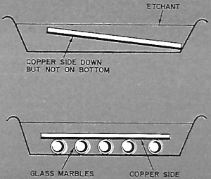
Fig. 9 - Place copper surface on glass marbles in a nonmetallic tray with etchant solution at a temperature of 90° to 120°, and agitate frequently.
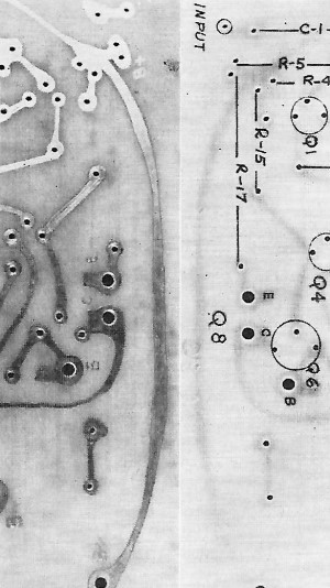
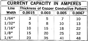
Fig. 10. When the etching process is complete, wash the board to remove all traces of etching solution. Then, before dismantling the mock-up board, mark location of each component with India ink. The table below can be used to figure optimum circuit line width. However, in no case should the path be narrower than 1/64 of an inch. The proper methods for terminating paths are shown in Fig. 7 When all paths have been covered with resist, and the ink has dried thoroughly, you will, at long last, be ready to make your first printed circuit board.
Incidentally, the author prefers, and recommends, the use of tape resist strips that are not only much simpler to apply, but which also give the finished circuit that certain professional appearance. Figure 8 shows "By-Buk" resist strips being applied, and the neat appearance certainly speaks for itself. To use tape resist, simply place the transfer sheet on which it comes, pigment side down, on the copper surface, and rub the back of the sheet with a pen or pencil to transfer the resist to the copper. Then the sheet is rolled back, and the resist stays stuck to the metal. With tape resists such as these, you can make attractive and functional boards without spending a single day in a drafting school. what's more, if you do make an error, you have only to scratch off the resist with a razor blade or pen knife. The Etching Process. The only thing we have to do now is mix the solution and etch away. Unless the etching solution provides instructions to the contrary, you will have to measure the circuit board surface area in inches to determine the amount of solution required. A good rule to follow is to use a pint of etchant for every 100 square inches of copper area. Drop a few glass marbles into the etching container to keep the circuit board from laying flat on the bottom. Then immerse the circuit board in the solution as shown in Fig. 9. Rock the container back and forth to agitate the solution until the excess copper has completely disappeared. The etching process will require approximately 20 to 30 minutes to complete and can be accelerated by heating the solution to approximately 150 degrees Fahrenheit. However, too rapid etching will produce serious undercutting below the resist. When the etching process is complete, the circuit board is washed to remove all traces of the etching solution. Varsol can be used to remove the resist, and the completed circuit is then burnished with fine steel wool to provide a clean copper surface for soldering. Your finished circuit board should look like Fig. 10, or better, if you used tape resist. Installing Components. To facilitate installation of the components, the location of each component is usually marked on the component side of the circuit board with India ink and identified by the reference designation of each part. When the marking is complete, the circuit board is ready to accept the components for mounting and soldering. Each component should be soldered in place individually even where two or more terminals join in a common land. Be careful when soldering etched circuit boards as the copper will lift from the surface of the board if too much heat is applied to it.
Posted March 27, 2018 |
|

 It's a good thing that
ferric chloride does not turn unstable and explosive after sitting in the dark for
many years or I might be in trouble. My bottle was bought back when
It's a good thing that
ferric chloride does not turn unstable and explosive after sitting in the dark for
many years or I might be in trouble. My bottle was bought back when