Do You Know Your Bipolar Transistors? - Part 1
|
|
Mr. Lothar Stern, of Motorola Semi, published a 3-part series on transistor theory in Popular Electronics magazine in 1973. This is part 1 (here is Part 2). By that time, transistors had pretty much replaced vacuum tubes in all new electronic products - if you don't count cathode ray tubes (CRTs) in televisions and some high power applications. Technical schools were still teaching about vacuum tubes since there was a still a lot of legacy equipment that needed to be maintained, and the main concentration had switched over to transistor theory. 1973, the year I turned 15, is right around the time I began seriously delving into the electrical and electronic realms as an eventual vocation. I distinctly remember being bewildered and amazed the first time I was told, in a USAF classroom, that a PN junction held to a fairly constant voltage (~0.7 V for silicon) regardless of the current through it - within the specified operational range. Here are Part 1, Part 2, and Part 3 (thanks to Jeff, KE5KQJ, for providing a copy of Part 3). Do You Know Your Bipolar Transistors? - Part 1
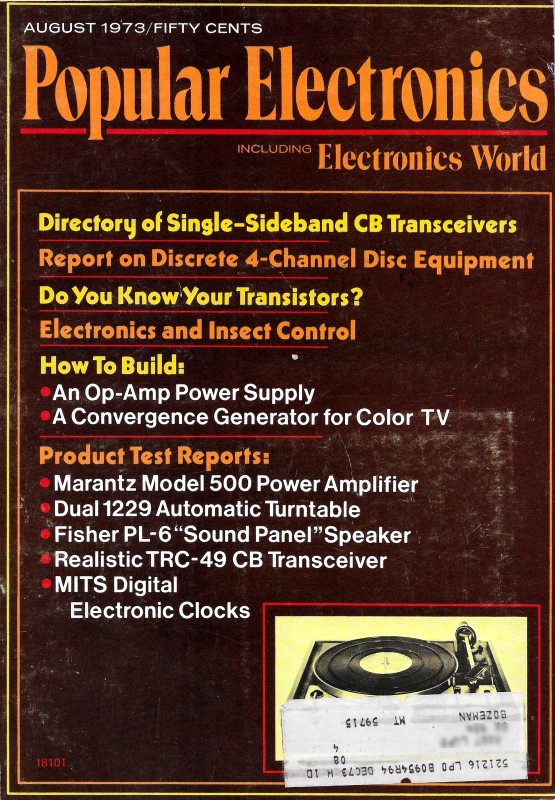
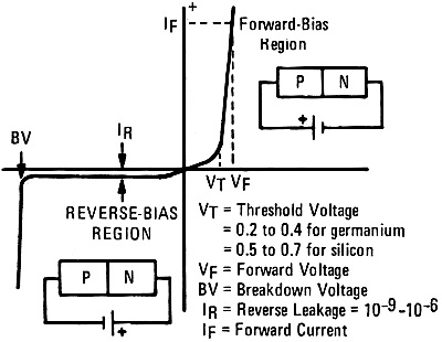
Fig. 1 - Forward and reverse characteristics of typical junction diode. Part 1 of a 3-Part Series on Basic Transistor Theory By Lothar Stern, Motorola Semiconductor Products Inc. The transistor is the most versatile component of the semiconductor family. Its most important characteristic is current and/or voltage amplification. Because of this capability, it is the heart of most solid-state electronic circuits involving signal amplification and switching. Transistor Types. There are two varieties of transistors: unipolar transistors, usually referred to as field-effect transistors (FET's), and bipolar transistors. The FET was invented circa 1930 but was not exploited commercially at the time. The bipolar transistor was invented around 1948 and rapidly became a practical product. The FET was finally developed as a commercial product by the early 1960's, many years after the bipolar transistor had already established itself. FET's, especially MOSFET's, are now used widely in low-noise front ends for TV and FM and are gaining importance in digital elements. However, in this article, we will discuss only bipolars. Transistor Basics. The basic element of any bipolar transistor is the pn junction, or diode, formed by chemically uniting a layer of p-doped semiconductor material with a layer of n-doped material. When the junction is forward biased (p layer positive, n layer negative), the current through the device increases rapidly as the voltage is increased. When the junction is reverse biased, an increase in voltage causes only a very small amount of leakage current, until the reverse voltage becomes high enough to cause "breakdown" of the junction. (See Fig. 1.) A transistor is formed by sandwiching a very thin layer of n-doped material between two layers of p-doped material (pnp transistor) or a thin layer of p-doped material between two layers of n-doped material (npn transistor). The characteristics of this 3-layer, 2-junction structure are achieved by varying the thickness and the resistivities and geometries of the three layers. Theoretically, an npn transistor should operate at higher frequencies than does a pnp device because electrons (the principal current carriers of an npn unit) are more mobile than holes (the principal current carriers of pnp devices). In practice, however, both types have similar characteristics. The main difference is that pnp transistors operate with a negative voltage on the collector element while npn transistors operate with a positive collector voltage. This makes it possible to have complementary circuits that often provide improved performance over the single-polarity circuits that can be implemented with only one type of transistor. The three layers of a bipolar transistor (Fig. 2) are the emitter, the base and the collector. The emitter represents the current source, where the current carriers originate. The base is the control element, and the collector is the element through which the current carriers are transferred to an external circuit.
Fig. 2 - Current flow in a transistor.
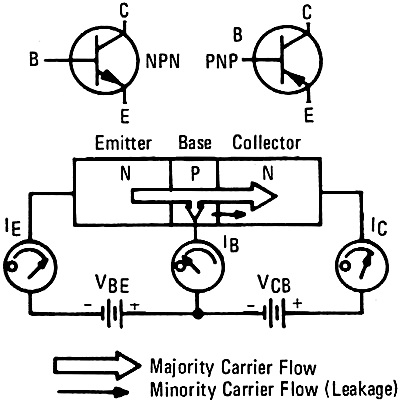
Fig. 3 - Three basic transistor circuits and their characteristic parameters.
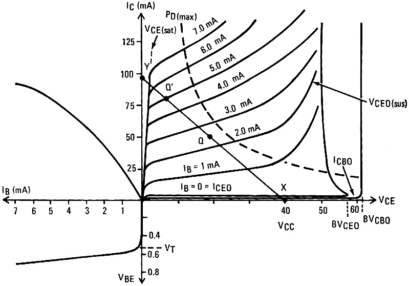
Fig. 4 - Characteristics of a common-emitter circuit showing the input and output. In operation, the collector-base junction is always reverse biased. If the emitter-base junction is forward biased, the emitter-base current is high, as in any forward biased diode junction. Instead of flowing out, however, most of this current diffuses through the very thin base region and crosses the collector-base junction, with only a small fraction flowing out the base lead. This action gives rise to the two commonly used expressions for current gain in a transistor. The first, a, is the ratio of IC/IE when the base-emitter junction is forward biased and is normally called the common-base current gain. It is always slightly less than unity (usually 0.95 to 0.998). The second gain expression is β, the ratio of IC/IB , called the common-emitter current gain. It can be quite high, depending on the value of α, since β = α/(1-α). Thus, if α = 0.95, β ≈ 20; and if α = 0.99, β ≈ 100. Circuit Configurations. There are three basic transistor circuit configurations: common emitter, common base, and common collector. They differ principally in the manner in which the signal is applied to the transistor and where the load is attached. Figure 3 shows these basic circuits. Since the common-emitter circuit is by far the most prevalent, most data sheets characterize the transistor in terms of this circuit. Figure 4 shows the characteristics of a typical transistor in a common-emitter circuit. The input circuit curve in quadrant III shows that a base-emitter voltage (VBE) of less than approximately 0.5 volt (for silicon; for germanium, about 0.2 volt) causes virtually no base or collector current to flow, thereby keeping the transistor cut off. Above 0.5 V, IB rises sharply, limited only by the ohmic resistance of the base region. Since the latter is very small, a very small rise in VBE (beyond the threshold voltage) causes a large rise in IB and IC as seen in quadrant II. From such a plot, the transistor current gain, IC/IB, can be established. It is also evident that considerable nonlinearity exists in the IC/IB curves. This indicates that distortion for large output signals can be quite high. The collector curves in quadrant I are the most significant. They show, for example, that the maximum reverse-bias collector voltage that can be applied, before breakdown of the collector-base junction, is BVCEO. The minimum collector voltage needed to keep the collector junction reverse biased, thereby sustaining transistor action, is VCE(sat). The maximum voltage excursion, therefore, is BVCEO - VCE(sat). When the transistor is cut off (IB = 0), a residual current, ICEO,, flows in the collector circuit. This leakage current can be reduced somewhat (but not to zero) by applying reverse bias to the emitter junction. The limiting value, with reverse bias applied to the emitter-base junction, is ICBO. This is equivalent to the collector-base leakage current when the emitter is open-circuited. Collector current increases rapidly as the base is energized. The maximum IC is that which would damage the internal transistor structure, This value of collector current is given as a maximum rating on data sheets. Thus, the output current could range from IC(max) to ICEO (or ICBO in the event of reverse bias), but usually IC islimited to a value far less than IC(max). Power dissipation, PD, is the product of VCE and IC and it causes the collector junction to heat up. Beyond a critical junction temperature, TJ(max), the device could be damaged. Thus the PD(max) rating of a transistor limits the maximum VCE and IC that can be applied simultaneously. The locus of a PD(max) rating is a parabolic curve on the VCE/IC plot. A load line, XQY, must be chosen to prevent steady-state operation to the right of the locus. From the above it is evident that, when the voltage applied between base and emitter is less than approximately 0.5 V, there is only a very small current flow through the transistor. Between collector and emitter, therefore, the transistor represents a very high resistance, or open switch. When VBE is raised above the threshold voltage, the internal resistance of the transistor drops to a very small value so that the device approximates a closed switch. As shown in Fig. 4, it takes a change of only 7 mA of IB along loadline XQY to cause VCE to change from VCC to VCE(sat), that is, from an open switch to a closed switch. This switch action is accomplished by a VBE of only a few tenths of a volt. (To be continued.)
Posted April 17, 2023 |
|