Tunnel Diodes
|
|
A decade after tunnel diodes were first invented by Nobel Laureate Leo Esaki, grand plans for the unique device never played out. Predictions included its use for computer solid state memories to replace magnetic core arrays. Tunnel diodes benefitted from the aura surrounding their exploitation of the quantum mechanical tunnelling phenomenon, which had a futuristic ring to it. Conventional diodes, having a relatively wide depletion region, require the current carriers (electrons and holes) to overcome a potential hill in traveling from the valence band to the conduction band of energies. Since high doping levels are used in the tunnel diode, a narrow depletion region is formed at the junction. This allows electrons to "tunnel" directly through from the valence to the conduction bands. It is this mechanism which gives rise to the tunnel-diode characteristics, including the negative-resistance region. This edition of Electronics World ran a series of diode articles: Hot Carrier Diodes, Variable-Capacitance Diodes, Tunnel Diodes, Microwave Power Diodes, A Survey of Silicon Junction Diodes, and Light-Emitting Diodes. Tunnel Diodes
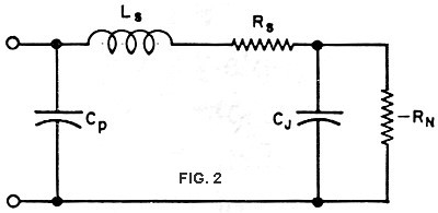
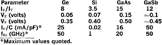
Following Esaki's announcement of the tunnel diode in 1958, expectations ran high for its potential use in a wide variety of applications. Many people thought that the tunnel diode would replace all magnetic cores and transistors in the digital computer. Because of the rapid progress made in conventional discrete diodes and transistors and the phenomenal development of integrated circuits, most of the early hopes never materialized. Taking advantage of its good frequency response and low noise characteristics, the greatest application of the tunnel diode today is for oscillators and amplifiers operating at video and microwave frequencies. The volume of sales for tunnel diodes was $4.5 million in 1968; by 1972 it is expected to reach close to $7 million. Leading manufacturers of tunnel diodes include Centralab, G-E, Motorola, Philco-Ford, RCA, Raytheon, Sylvania, and Texas Instruments. In quantities from 1 to 99, prices range from $1 to $15, depending on device characteristics. A typical tunnel diode characteristic curve and schematic symbol are shown in Fig. 1. Between peak and valley voltages VP and VV, respectively (corresponding to peak and valley currents IP and IV), diode current decreases with increasing diode voltage. This behavior results in the region of negative resistance -RN, which permits the tunnel diode to be used as a switch, oscillator, or amplifier. Conventional diodes, having a relatively wide depletion region, require the current carriers (electrons and holes) to overcome a potential hill in traveling from the valence band to the conduction band of energies. Since high doping levels are used in the tunnel diode, a narrow depletion region is formed at the junction. This allows electrons to "tunnel" directly through from the valence to the conduction bands. It is this mechanism which gives rise to the tunnel-diode characteristics, including the negative-resistance region. For voltages exceeding the valley voltage, the tunnel diode assumes the characteristics of the conventional p-n junction diode, A small-signal model of the device is shown in Fig, 2. Capacitance CJ represents junction capacitance; CP is the package capacitance. Series resistance RS is ohmic and LS is the lead inductance. The negative resistance is denoted by -RN. Typical values of these parameters for a tunnel diode with a peak current rating of 10 mA are: LS ≈ 5 nH, RS ≈ 1 ohm, -RN ≈ -25 ohms, and CJ ≈ 10-20 pF. CP depends on the mounting and packaging. Four basic materials used for fabricating tunnel diodes are: germanium (Ge), silicon (Si), gallium arsenide (GaAs), and gallium antimonide (GaSb), Typical values of significant tunnel-diode parameters are listed in the table. Besides the peak-to-valley current ratio IP/IV and the peak and valley voltages VP and VV, two other parameters of interest are included: the peak current-to-capacitance ratio IP/C (where C is the sum of the junction and package capacitance) and the resistive cut-off frequency fR0 (the frequency at which the net negative resistance reduces to zero). These two parameters serve as figures of merit for tunnel diodes.
Because of their low noise, gallium antimonide and germanium diodes are generally employed for amplifiers. Although germanium exhibits somewhat greater noise than gallium antimonide, germanium tunnel diodes are more stable with respect to temperature. Gallium arsenide diodes exhibit the greatest power-output capabilities and are therefore invariably used for oscillators. For high-speed switching, gallium arsenide and germanium tunnel diodes are best. Silicon, however, would be required at elevated temperatures (up to 150°C). Referring to Fig. 1A, if the forward characteristic is altered to appear as shown in Fig. 3A, the characteristics of the back diode are obtained. Interchanging the first and third quadrants results in Fig. 3B. An examination of the "forward" characteristics in quadrant I of Fig. 3B reveals that the cut-in or threshold voltage is approximately zero volts. The new reverse characteristic is not too different from that of ordinary diodes. At room temperature, the cut-in voltage is 0.6 and 0.2 V for silicon and germanium p-n junction diodes, respectively. Therefore, back diodes are well suited for rectifying very low-amplitude signals; they are also used as video detectors in microwave applications. Some companies making back diodes are G-E, Sylvania, and Transitron. In small quantities prices are about $3 and up.
Posted February 19, 2018 |
|


 Tunnel diodes exhibit good resistance to radiation.
The valley current is most sensitive, with significant changes in its value occurring
in the vicinity of an integrated' flux density of 1016 neutrons/cm2.
The peak and valley voltages have negative temperature coefficients of 0.1 and 0.8 mV/°C,
respectively. Typical variation of IP and VP over a temperature
range of -55°C to 150°C is 10 percent. The valley current is temperature sensitive;
its value at 150°C may be 3 times as great as at -55°C.
Tunnel diodes exhibit good resistance to radiation.
The valley current is most sensitive, with significant changes in its value occurring
in the vicinity of an integrated' flux density of 1016 neutrons/cm2.
The peak and valley voltages have negative temperature coefficients of 0.1 and 0.8 mV/°C,
respectively. Typical variation of IP and VP over a temperature
range of -55°C to 150°C is 10 percent. The valley current is temperature sensitive;
its value at 150°C may be 3 times as great as at -55°C.