Evolution in Electronics: Integrated Circuits
|
|
Sixty years ago when this "Evolution in Electronics: Integrated Circuits" article appeared in Electronics World magazine, commercially manufactured (as opposed to in laboratories and small volume production) ICs were at the very beginning of their evolutionary lifetime. It was only 14 years earlier that the transistor's invention first been announced at Bell Labs. Jack Kilby, of Texas Instruments, is credited with having built the first practical integrated circuit in 1958. The Darlington transistor IC was a relatively simple achievement since there were no passive components on the die. A 2−stage amplifier, as shown in figures 2 and 4, with on-chip resistors and capacitors was a big deal at the time. Evolution in Electronics: Integrated Circuits
A new manufacturing technique in which an entire circuit is fabricated without using conventional components. Small size, more reliability, longer life, reduced costs are the results. We are witnessing today an evolution in the field of electronics whose impending impact on the industry promises to eclipse even the dramatic changes brought about by the invention of the transistor some years ago. This time, however, it is not the invention of a new product that will vitally affect the shape of things to come. Rather, it is the development of a new concept in manufacturing - a technique known as "integrated circuits." In its ultimate form, the technology of integrated circuits represents a complete departure from current equipment design and manufacturing techniques. The conventional building blocks of electronics - resistors, capacitors, and inductors - will virtually disappear as separate entities. Their specific functions will be accomplished by microscopically small depositions or growths of material layers, or films, which may be individually unrecognizable and inseparable from a complete circuit. In fact, the entire complex electronic circuit will be so thoroughly united that the complete circuit function, rather than today's individual parts, will become the basic component of tomorrow's electronic equipment. And the process will yield advantages that past techniques cannot possibly duplicate.
Fig. 1 - Schematic diagram of Darlington type amplifier utilizing five direct-coupled stages. The total gain available is usually much higher than normally required so that the output is usually taken from one of the earlier stages of the amplifier.
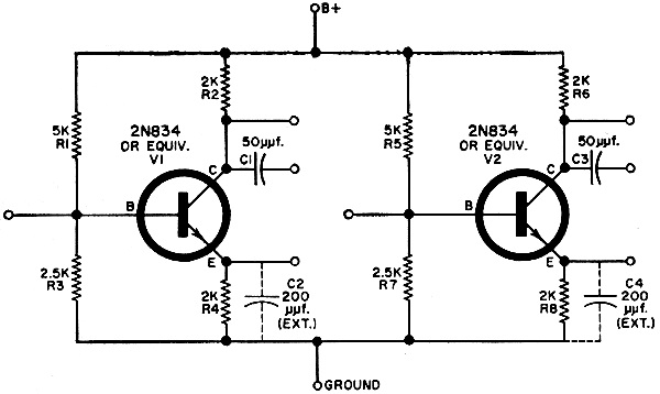
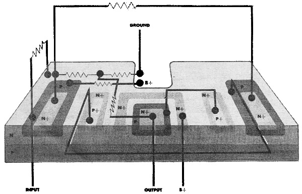
Fig. 2 - Schematic diagram of two-stage RC-coupled amplifier.
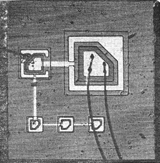
Fig. 3 - Greatly enlarged view of 5-stage Darlington amplifier which is to be mounted between the pins of a typical transistor header. Output may be taken from any stage, hence offering various amounts of amplification from a single integrated unit. The erstwhile rack of complex equipment, which the transistor has already reduced to single-drawer size, will be further diminished to matchbox proportions. The equipment will require only a small fraction of the operating power now needed for similar applications, and an increase in reliability by an order of magnitude is a conservative prediction. And finally, the processes of integrated circuits will eventually permit price reductions that will not only accelerate the logarithmic spiral of electronic progress but can open new areas of applications for every conceivable electronics market. To appreciate the advantages of integrated circuits, let us take a close look at a very simple type of structure. Figures 1 and 3 show a typical 5-stage Darlington amplifier - a direct-coupled amplifier in which the output of one stage is connected directly to the input of the next - in schematic and integrated circuit form respectively. The actual circuit, too small to be analyzed with the naked eye, is shown, greatly enlarged in Fig. 3. The entire circuit, which is fabricated on a tiny chip of material less than one-sixteenth of an inch square, is then mounted between two pins of a standard transistor header. Since the header serves merely as a means for interconnecting this circuit with others in the complete equipment, it is quite possible, with a different packaging technique, to produce a unit whose total size is only little larger than the volume of the "chip" itself. Actually, a direct-coupled amplifier is quite easy to fabricate since it involves only the interconnection of a number of active elements. A far more complex type of circuit is one combining both active and passive elements on a single substrate. Yet, even these have been fabricated successfully. The schematic diagram of such an amplifier, Fig. 2, shows two complete RC-coupled amplifier stages although there is no connection between the stages themselves. Rather, the input and output terminals of each stage are brought out to separate pins of a transistor header so that the circuit designer may employ either one or two stages, depending on his amplification requirements. This fabrication technique adds considerable flexibility to the completed device since the second stage adds little or nothing to the cost of the final device, thus permitting the same unit to be used as either a single-stage or two-stage amplifier. Fig. 4 shows a detailed drawing of the circuit pattern which permits correlation between the equivalent "pattern parts" and those shown on the schematic diagram. Advantages of Integrated Circuits From the foregoing it is quite apparent that the development of integrated circuits will produce an impressive reduction of size and weight in the over-all equipment. When the space-saving feature of a single integrated circuit is multiplied by a number of separate circuits, all of which can be mounted in a single transistor-type case, as in Figs. 5 and 6, the equivalent of 50 to 100 individual parts will occupy no more room than a single transistor. But, important as this space- and weight-saving feature may be, it is only secondary to the far greater advantages of reduced cost, greater reliability, and improved performance which integrated circuits will eventually provide. Reducing Circuit Costs In today's skyrocketing technology it is no longer a question of "can we develop an advanced electronic system," but rather "can we afford to develop a particular system." The increasing complexities and the mounting materials and labor costs associated with today's more sophisticated electronic equipment are already placing a heavy burden on our ability to pay the price for continuing progress. The anticipated cost-reducing features of integrated circuits, therefore, may well be their most important advantage. True, the cost of many presently available integrated circuits is quite high compared with identical circuits made in the conventional manner, but that is primarily because the former are fabricated in relatively small quantities for sampling purposes. As integrated circuits move from the experimental to the production stage the pricing pattern for off-the-shelf units in quantity should follow that of transistors in recent years.
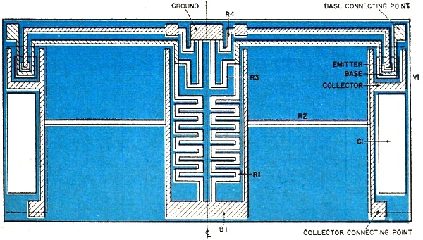
Fig. 4 - Integrated circuit pattern of 2-stage amplifier with the various "components" labeled. Notice that the left-hand side of the pattern is a mirror image of the right side pattern.
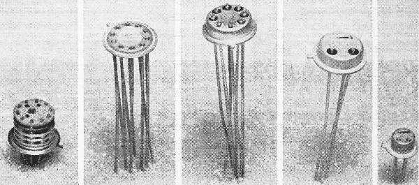
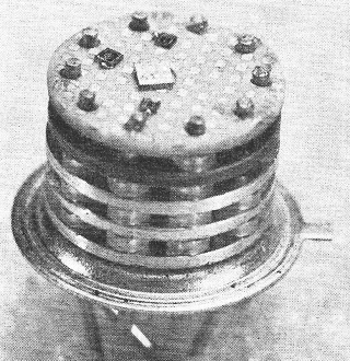
Fig. 5 - Various transistor headers used for mounting circuits.
Fig. 6 - Enlargement of unit shown at left in Fig. 5 shows four separate circuit layers capable of housing four isolated circuits with the equivalent of up to one hundred separate components. There is good reason why this should be so. With the proper pattern and masks, two transistors, or even a dozen, can be fabricated on a single chip in the same amount of time and with virtually the same quantity of material as a single unit. Diodes, resistors, capacitors, and even small inductors can be deposited on the same substrate with the same processes used for the fabrication of transistors. Thus, the manufacture of complete circuits, in the long run, should be little more expensive than the cost of fabricating a single transistor at the present time. Considering the fact that hundreds of circuits can often be deposited on a single wafer, and that dozens of wafers can be processed simultaneously, Fig. 7, the cost advantages of integrated circuits become readily apparent. Improved Reliability With the ever-increasing demands made on modern electronic equipment, the reliability of individual components may well be the limiting factor as to the ultimate complexity that can be designed into a particular system. Consider, for example, a component that has a failure rate of 1% per thousand hours of operation. If a system is designed to use 100 such components, it is a reasonable assumption that one of these will fail after 1000 hours of operation causing the equipment to malfunction. A system using 1000 components can be expected to fail after only 100 hours and another utilizing 10,000 components is likely to quit functioning after only 10 hours of operation. Thus, in the expanding technology it is possible to design a system so complex that it will perform every conceivable function-but which uses so many parts that it will be impossible to keep it in operation. Before the development of the transistor, the active elements - vacuum tubes - normally represented the most unreliable component in electronic equipment. Because of their relatively high failure rate, they were plugged into sockets so that they could be replaced easily and quickly in the event of failure. With transistorization, the picture has changed radically. Transistors are often wired directly into a circuit because, in the event of circuit failures, they are the last components to be suspected of causing the trouble. In integrated circuitry, passive elements such as resistors and capacitors can be made by exactly the same processes used in the manufacture of semiconductor devices. Their anticipated failure rate, therefore, is no greater than that of the most reliable components producible in today's technology. Moreover, with integrated circuits the maze of interconnecting wires which characterizes conventional equipment and is the cause of a good percentage of equipment failures is substantially reduced. Within each circuit the various elements are deposited in adjacent and superimposed layers for which no separate connections are required. This feature alone causes a substantial reduction in potential trouble spots. Improved Performance Improved performance today is virtually synonymous with increased circuit speed. It is this aspect of the equipment that permits us to utilize higher frequencies and to increase the scope of operation of electronic computers. And, until recently, the capabilities of individual components represented the limiting factors in the ultimate attainable equipment speed. Recent improvements in components, however, have resulted in some systems in which the propagation delay - in actual time required for electrons to travel from one point of a system to another - prohibits faster operation. While a transistor is able to switch at a rate of only a few nanoseconds (a few millimicroseconds), it actually may require more time for a signal to travel from the input to the output of a large computer due to the physical separation of components. Only a reduction of equipment size can pierce the speed-size ceiling to permit substantial improvements in performance. Integrated circuits are the obvious answer to shorter propagation delays. The lack of physical separation of parts within a given circuit, coupled with the close spacing between separate circuits which considerably reduces wiring parasitics, promise a significant improvement in the speed-complexity product to meet the demands of tomorrow's equipment. Evolution of Circuit Technology The realization of integrated circuit advantages is based on a technology which represents a radical departure from the well-known design and construction concepts associated with the electronics art. Although the past decade has seen repeatedly successful efforts toward reducing the size and weight of electronic equipment-including miniaturization, subminiaturization, and finally microminiaturization - all of these were based on the principle of using separate parts, individually connected through wires or printed circuit patterns, to form a complete circuit. "Miniaturization," for example, was merely a concerted effort to reduce the size and weight of the separate passive circuit elements to parallel the size reductions precipitated by a switch from tubes to transistors. The popular shirt-pocket transistor radio attests to the success of this project. But miniaturization was only the first step in overcoming the problems of an increasingly size-conscious science. To compress the size of equipment still further, or to increase the complexity of the circuits that could be squeezed into a given volume, parts were again decreased in size in a stage of "subminiaturization" which retained the general shape of the parts but, in some cases, led to unique assembly techniques. The "cordwood" technique, in which cylindrical axial-lead components are stacked, with their leads fed through matched holes in parallel printed-circuit boards mounted in front of and behind the stack, is a good example. Finally, in the ultimate size reducing process of "microminiaturization," tiny pill-type parts were pressed into equally small recesses in circuit boards and interconnected by printed wiring. This, for the first time, represented a departure from the conventional shape and form factor of the familiar parts. Yet, all three size-reducing steps had one thing in common - the circuit designer still retained uninhibited freedom of choice in the number of parts and parts values of the individual components. Integrated Circuit Approach
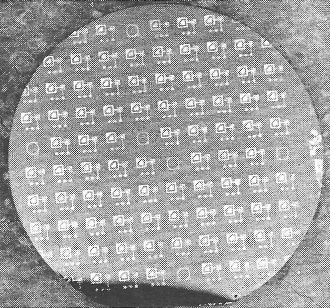
Fig. 7 - Large numbers of integrated circuits are normally deposited or grown simultaneously through "masks" on thin silicon wafers. The wafers are then scribed and broken to yield up to several hundred separate circuits ready for mounting and bonding to a conventional transistor header or case.
Fig. 8 - Top view showing a stair-step voltage generator made up of 20 micro-transistors, 34 micro-diodes, and all associated passive elements, most made by thin-film processes.
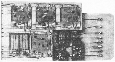
Fig. 9 - Wide-band video amplifier composed of 3 transistors, 2 zener diodes, and 6 resistors. Both semiconductor and passive thin-film techniques are employed. With this approach, all active elements can be fabricated on a single semiconductor substrate and interconnected with passive elements on a passive substrate in a stacked header arrangement shown in Fig. 6. The development of a thin-film capability represented the first real advance from the separate-parts techniques to current integrated circuit concepts. With thin films it is possible, by means of evaporation and anodization processes, to duplicate the functions of separate resistors, capacitors, and inductors with chemical layers of material deposited on a glass or ceramic substrate. Interconnections, made by overlapping or touching films, form a pattern of passive elements associated with a particular circuit. For the first time, the circuit designer found himself working with geometric patterns and configurations, rather than actual physical parts, in developing his circuit. But in so doing, he achieved not only additional size reduction, but gained an anticipated increase in reliability through the elimination of separately interconnected parts. Thin-film circuits, however, do not lend themselves to complete circuit integration. As yet, none of the many companies working in the field has perfected a means for depositing thin-film diodes or transistors - the active elements - on a glass or ceramic substrate. Complete thin-film circuits, therefore, combine thin-film passive patterns with microminiature, separately connected active components, as shown in Fig. 8. The answer to truly integrated circuits lies in the more recent development of a semiconductor integrated circuit technology which combines thin-film passive parts with active elements on or within a single crystal semiconductor substrate. Already, processes have been developed which permit the deposition of resistance values ranging from a few ohms to several megohms, and capacitors to 0.01 μf. on such substrates by methods completely compatible with the fabrication of active elements. Thus, it is possible, as discussed earlier, to literally grow a complete circuit in a single, compatible fabrication process. But semiconductor integrated circuits, too, have their limitations. It is difficult, for example, to obtain the required degree of electrical isolation between parts associated with certain circuits. Since all parts are fabricated within a semiconductor block, circuits of this nature are limited at present to configurations that can tolerate relatively high parasitic capacitance coupling between parts. Thus it is a matter of designing circuits that are tolerant of intercomponent coupling, or of combining passive thin-film concepts with semiconductor technology for the fabrication of more complex circuits, as visualized in Fig. 9. It is this combined approach that may well be employed for more complex integrated circuits in the immediate future. Nevertheless, a wide variety of integrated circuits has already been produced by the semiconductor technique alone. These run the gamut from digital switching and logic elements - including flip-flops, "nor" and "nand" gates, etc. - to linear elements including both high- and low-frequency amplifiers. They are practical circuits that are being sampled by the industry for possible design in tomorrow's equipment. And, although relatively simple, they are indicative of the progress that can be expected. Epitaxial growth techniques, developed for growing crystals of highly controllable resistivities in selective patterns, are being employed to attack the isolation problems with encouraging results. Advanced methods of diffusion are being investigated and show promise of increasing isolation factors. It seems only a matter of time - a relatively short time - before more complex, truly integrated circuits can be fabricated to order in any desired quantity. Opportunities in Integrated Electronics The total impact of integrated circuits on the electronics society, far reaching as it may be, is not as immediate as it may appear on the surface. It must be remembered that the transistor displaced the vacuum tube in many possible applications only after 1.5 years of maturity. The infiltration of integrated circuits into the over-all economy is expected to follow a similar timetable. It is anticipated that they will live compatibly alongside transistors and even vacuum tubes for a good many years. The reason for this is that the advantages of integrated circuits have, in many instances, outdistanced the present requirements. Although an improvement in reliability is of vital importance ill many military systems, the present reliability of transistors, for example, is ample for the majority of applications. While the space- and weight-saving aspect of integrated circuits is mandatory for our unfolding space program, it is of little importance for TV sets, for instance, where the demand for ever-increasing picture tube sizes limits the minimum dimensions of the ultimate package. Even the cost-reducing features of integrated circuits are at present limited to special applications, such as computers, where only the need for thousands of similar circuits demands the production quantities necessary for low-cost fabrication. Thus, while integrated circuits may eventually obsolete a number of job classifications currently in demand, in the immediate future they will create an unprecedented demand for physicists, metallurgists, chemists, and semiconductor engineers needed to further develop the state of this art. Even circuits engineers will be in increasing demand, although an important premium will be placed on circuit designers with considerable training or experience in one or more of the above-mentioned sciences. The reason is that integrated circuits designers must be thoroughly familiar with electronic circuits per se, but also with the fabrication procedures and characteristics of semiconductor processes. A particular circuit may be reproducible with discrete thin-film capacitors, yet it may be far less expensive and more efficient to fabricate the same circuit using the capacitive effect of a back-biased diode for the same purpose. The reduction of conventional circuits to integrated circuit form requires a specialized knowledge which opens new technical frontiers and increasing employment opportunities. Integrated Engineering But as the art of integrated circuits advances, the concept of engineering likewise will become more integrated, Today there are three broad and distinctly separate engineering categories - components engineering, circuits design, and systems engineering. The components engineer concerns himself only with the development of a range of component values which will become the tools of the circuit designer. He need not concern himself with the actual circuits nor does he require all intimate knowledge of the eventual application of his products. The circuit designer, on the other hand, cares little about the component fabrication process as long as a particular part has the electrical characteristics to fit his circuit requirement. He does not even have to concern himself with the needs of the systems engineer but can concentrate primarily on the development of circuits. Finally, the systems engineer treats the output of the circuit designer as his particular components, or building blocks, from which to construct a more complex system. In this technology, therefore, the three engineers can work virtually independent of each other, neither knowing nor caring about the work of the other. Not so with integrated circuits. Here is an entirely new technology that demands the very closest cooperation among all phases of electronics engineering. The circuit designer now becomes the focal point of a team that must become almost as integrated as the circuits themselves. Not only must he acquaint himself with the various fabrication procedures for integrated circuit parts - since parts made by different methods such as diffusion, epitaxial growth, alloying, etc. may exhibit different electrical characteristics - he must also be thoroughly familiar with the end product. For integrated circuits are no longer an assortment of individual, easily replaceable parts, but rather a series of irreparable entities that, ultimately, will have to be designed to fit the specific needs of the final system. No longer can the circuit designer afford the luxury of designing a general circuit, hoping to modify it later for a specific requirement. Since the cost-reducing feature of integrated circuits lies in quantity production, and since most of the total cost is in the development of the first trouble-free production sample (virtually hundreds of identical circuits can be made almost as cheaply as a single unit) each circuit must be designed with the end product in mind. It is anticipated that the systems engineer can design his system only after consultation with the circuit designer who determines the type of circuits to be used and the packaging techniques that can be employed. Both, however, will depend, to a great extent, on the components "process" engineer whose intimate knowledge of fabrication processes and capabilities must guide the design of both circuits and systems. The components man, therefore, must be almost as familiar with circuit requirements as with his own particular specialty. Although the field of integrated circuits still has its specialists, each must have a working knowledge of the problems and objectives of the other. The principal rewards of this new field will be reaped only by men with that high order of initiative needed to meet the challenge of this vital new technology.
Posted November 2, 2022 |
|
 By Lother Stern, Motorola Semiconductor Products
Inc.
By Lother Stern, Motorola Semiconductor Products
Inc.