Module 8 - Introduction to Amplifiers: Coupling
|
||||||||||||||||||||||||||||||||||||||||||||||||||
|
Module 8 − Introduction to Amplifiers Pages i, 1−1, 1−11, 1−21, 1−31, 2−1, 2−11, 2−21, 2−31, 3−1, 3−11, 3−21, 3−31, 3−41, 3−51, 3−61, AI−1, Index
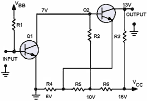
Notice that the output (collector) of Q1 is connected directly to the input (base) of Q2. The network of R4, R5, and R6 is a voltage divider used to provide the bias and operating voltages for Q1 and Q2. The entire circuit provides two stages of amplification.
Figure 1-9 - Direct-coupled transistor amplifiers.
Figure 1-10 - RC-coupled transistor amplifier. Direct coupling provides a good frequency response since no frequency-sensitive components (inductors and capacitors) are used. The frequency response of a circuit using direct coupling is affected only by the amplifying device itself. Direct coupling has several disadvantages, however. The major problem is the power supply requirements for direct-coupled amplifiers. Each succeeding stage requires a higher voltage. The load and voltage divider resistors use a large amount of power and the biasing can become very complicated. In addition, it is difficult to match the impedance from stage to stage with direct coupling. (Impedance matching is covered a little later in this chapter.) The direct-coupled amplifier is not very efficient and the losses increase as the number of stages increase. Because of the disadvantages, direct coupling is not used very often. RC Coupling The most commonly used coupling in amplifiers is RC coupling. An RC-coupling network is shown in figure 1-10. The network of R1, R2, and C1 enclosed in the dashed lines of the figure is the coupling network. You may notice that the circuitry for Q1 and Q2 is incomplete. That is intentional so that you can concentrate on the coupling network. R1 acts as a load resistor for Q1 (the first stage) and develops the output signal of that stage. Do you remember how a capacitor reacts to ac and dc? The capacitor, C1, "blocks" the dc of Q1's collector, but "passes" the ac output signal. R2 develops this passed, or coupled, signal as the input signal to Q2 (the second stage). This arrangement allows the coupling of the signal while it isolates the biasing of each stage. This solves many of the problems associated with direct coupling. RC coupling does have a few disadvantages. The resistors use dc power and so the amplifier has low efficiency. The capacitor tends to limit the low-frequency response of the amplifier and the amplifying device itself limits the high-frequency response. For audio amplifiers this is usually not a problem; techniques for overcoming these frequency limitations will be covered later in this module. Before you move on to the next type of coupling, consider the capacitor in the RC coupling. You probably remember that capacitive reactance (X C) is determined by the following formula:
This explains why the low frequencies are limited by the capacitor. As frequency decreases, XC increases. This causes more of the signal to be "lost" in the capacitor. The formula for XC also shows that the value of capacitance (C) should be relatively high so that capacitive reactance (XC) can be kept as low as possible. So, when a capacitor is used as a coupling element, the capacitance should be relatively high so that it will couple the entire signal well and not reduce or distort the signal. Impedance Coupling Impedance coupling is very similar to RC coupling. The difference is the use of an impedance device (a coil) to replace the load resistor of the first stage.
Figure 1-11 - Impedance-coupled transistor amplifier.
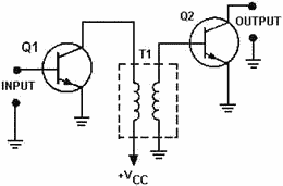
Figure 1-12 - Transformer-coupled transistor amplifier. Figure 1-11 shows an impedance-coupling network between two stages of amplification. L1 is the load for Q1 and develops the output signal of the first stage. Since the d.c. resistance of a coil is low, the efficiency of the amplifier stage is increased. The amount of signal developed in the output of the stage depends on the inductive reactance of L1. Remember the formula for inductive reactance: The formula shows that for inductive reactance to be large, either inductance or frequency or both must be high. Therefore, load inductors should have relatively large amounts of inductance and are most effective at high frequencies. This explains why impedance coupling is usually not used for audio amplifiers. The rest of the coupling network (C1 and R1) functions just as their counterparts (C1 and R2) in the RC-coupling network. C1 couples the signal between stages while blocking the d.c. and R1 develops the input signal to the second stage (Q2). Transformer Coupling Figure 1-12 shows a transformer-coupling network between two stages of amplification. The transformer action of T1 couples the signal from the first stage to the second stage. In figure 1-12, the primary of T1 acts as the load for the first stage (Q1) and the secondary of T1 acts as the developing impedance for the second stage (Q2). No capacitor is needed because transformer action couples the signal between the primary and secondary of T1. The inductors that make up the primary and secondary of the transformer have very little dc resistance, so the efficiency of the amplifiers is very high. Transformer coupling is very often used for the final output (between the final amplifier stage and the output device) because of the impedance-matching qualities of the transformer. The frequency response of transformer-coupled amplifiers is limited by the inductive reactance of the transformer just as it was limited in impedance coupling. Q-12. What is the purpose of an amplifier-coupling network? Q-13. What are four methods of coupling amplifier stages? Q-14. What is the most common form of coupling? Q-15. What type coupling is usually used to couple the output from a power amplifier? Q-16. What type coupling would be most useful for an audio amplifier between the first and second stages? Q-17. What type of coupling is most effective at high frequencies? Impedance Considerations for Amplifiers It has been mentioned that efficiency and impedance are important in amplifiers. The reasons for this may not be too clear. You have been shown that any amplifier is a current-control device. Now there are two other principles you should try to keep in mind. First, there is no such thing as "something for nothing" in electronics. That means every time you do something to a signal it costs something. It might mean a loss in fidelity to get high power. Some other compromise might also be made when a circuit is designed. Regardless of the compromise, every stage will require and use power. This brings up the second principle-do things as efficiently as possible. The improvement and design of electronic circuits is an attempt to do things as cheaply as possible, in terms of power, when all the other requirements (fidelity, power output, frequency range, etc.) have been met.
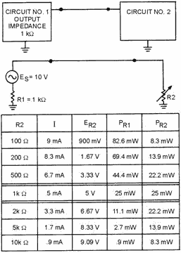
Figure 1-13 - Effect of impedance matching in the coupling of two circuits. This brings us to efficiency. The most efficient device is the one that does the job with the least loss of power. One of the largest losses of power is caused by impedance differences between the output of one circuit and the input of the next circuit. Perhaps the best way to think of an impedance difference (mismatch) between circuits is to think of different-sized water pipes. If you try to connect a one-inch water pipe to a two-inch water pipe without an adapter you will lose water. You must use an adapter. An impedance-matching device is like that adapter. It allows the connection of two devices with different impedances without the loss of power. Figure 1-13 shows two circuits connected together. Circuit number 1 can be considered as an a.c. source (ES) whose output impedance is represented by a resistor (R1). It can be considered as an a.c. source because the output signal is an a.c. voltage and comes from circuit number 1 through the output impedance. The input impedance of circuit number 2 is represented by a resistor in series with the source. The resistance is shown as variable to show what will happen as the input impedance of circuit number 2 is changed. The chart below the circuit shows the effect of a change in the input impedance of circuit number 2 (R2) on current (I), signal voltage developed at the input of circuit number 2 (ER2), the power at the output of circuit number 1 (PR1), and the power at the input to circuit number 2 (PR2). Two important facts are brought out in this chart. First, the power at the input to circuit number 2 is greatest when the impedances are equal (matched). The power is also equal at the output of circuit number 1 and the input of circuit number 2 when the impedance is matched. The second fact is that the largest voltage signal is developed at the input to circuit number 2 when its input impedance is much larger than the output impedance of circuit number 1. However, the power at the input of circuit number 2 is very low under these conditions. So you must decide what conditions you want in coupling two circuits together and select the components appropriately. Two important points to remember about impedance matching are as follows. (1) Maximum power transfer requires matched impedance. (2) To get maximum voltage at the input of a circuit requires an intentional impedance mismatch with the circuit that is providing the input signal.
Figure 1-14 - Transistor amplifier configurations and their impedance characteristics.
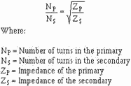
Impedance Characteristics of Amplifier Configurations Now that you have seen the importance of impedance matching the stages in an electronic device, you may wonder what impedance characteristics an amplifier has. The input and output impedances of a transistor amplifier depend upon the configuration of the transistor. In Module 7, Introduction to Solid-State Devices and Power Supplies, you were introduced to the three transistor configurations; the common emitter, the common base, and the common collector. Examples of these configurations and their impedance characteristics are shown in figure 1-14. Note: Only approximate impedance values are shown. This is because the exact impedance values will vary from circuit to circuit. The impedance of any particular circuit depends upon the device (transistor) and the other circuit components. The value of impedance can be computed by dividing the signal voltage by the signal current. Therefore: The common-emitter configuration provides a medium input impedance and a medium output impedance. The common-base configuration provides a low input impedance and a high output impedance. The common-collector configuration provides a high input impedance and a low output impedance. The common-collector configuration is often used to provide impedance matching between a high output impedance and a low input impedance. If the amplifier stage is transformer coupled, the turns ratio of the transformer can be selected to provide impedance matching. In NEETS Module 2, Introduction to Alternating Current and Transformers, you were shown the relationship between the turns ratio and the impedance ratio in a transformer. The relationship is expressed in the following formula:
As you can see, impedance matching between stages can be accomplished by a combination of the amplifier configuration and the components used in the amplifier circuit.
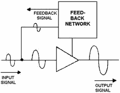
Figure 1-15 - Positive feedback in an amplifier.
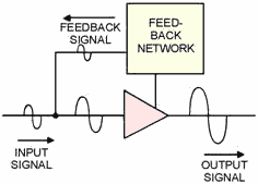
Figure 1-16 - Negative feedback in an amplifier.
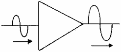
Figure 1-17A-Feedback uses in amplifiers.
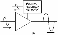
Figure 1-17B - Feedback uses in amplifiers.
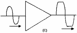
Figure 1-17C - Feedback uses in amplifiers.
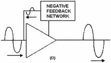
Figure 1-17D - Feedback uses in amplifiers. Q-18. What impedance relationship between the output of one circuit and the input of another circuit will provide the maximum power transfer? Q-19. If maximum current is desired at the input to a circuit, should the input impedance of that circuit be lower than, equal to, or higher than the output impedance of the previous stage? Q-20. What are the input- and output-impedance characteristics of the three transistor configurations? Q-21. What transistor circuit configuration should be used to match a high output impedance to a low input impedance? Q-22. What type of coupling is most useful for impedance matching? Amplifier Feedback Perhaps you have been around a public address system when a squeal or high-pitched noise has come from the speaker. Someone will turn down the volume and the noise will stop. That noise is an indication that the amplifier (at least one stage of amplification) has begun oscillating. Oscillation is covered in detail in NEETS Module 9, Introduction to Wave-Generation and Wave-Shaping Circuits. For now, you need only realize that the oscillation is caused by a small part of the signal from the amplifier output being sent back to the input of the amplifier. This signal is amplified and again sent back to the input where it is amplified again. This process continues and the result is a loud noise out of the speaker. The process of sending part of the output signal of an amplifier back to the input of the amplifier is called Feedback. There are two types of feedback in amplifiers. They are Positive Feedback, also called Regenerative Feedback, and Negative Feedback, also called Degenerative Feedback. The difference between these two types is whether the feedback signal is in phase or out of phase with the input signal. Positive feedback occurs when the feedback signal is in phase with the input signal. Figure 1-15 shows a block diagram of an amplifier with positive feedback. Notice that the feedback signal is in phase with the input signal. This means that the feedback signal will add to or "regenerate" the input signal. The result is a larger amplitude output signal than would occur without the feedback. This type of feedback is what causes the public address system to squeal as described above. Figure 1-16 is a block diagram of an amplifier with negative feedback. In this case, the feedback signal is out of phase with the input signal. This means that the feedback signal will subtract from or "degenerate" the input signal. This results in a lower amplitude output signal than would occur without the feedback. Sometimes feedback that is not desired occurs in an amplifier. This happens at high frequencies and limits the high-frequency response of an amplifier. Unwanted feedback also occurs as the result of some circuit components used in the biasing or coupling network. The usual solution to unwanted feedback is a feedback network of the opposite type. For example, a positive feedback network would counteract unwanted, negative feedback. Feedback is also used to get the ideal input signal. Normally, the maximum output signal is desired from an amplifier. The amount of the output signal from an amplifier is dependent on the amount of the input signal. However, if the input signal is too large, the amplifying device will be saturated and/or cut off during part of the input signal. This causes the output signal to be distorted and reduces the fidelity of the amplifier. Amplifiers must provide the proper balance of gain and fidelity. Figure 1-17 shows the way in which feedback can be used to provide the maximum output signal without a loss in fidelity. In view A, an amplifier has good fidelity, but less gain than it could have. By adding some positive feedback, as in view B, the gain of the stage is increased. In view C, an amplifier has so much gain and such a large input signal that the output signal is distorted. This distortion is caused by the amplifying device becoming saturated and cutoff. By adding a negative feedback system, as in view D, the gain of the stage is decreased and the fidelity of the output signal improved. Positive and negative feedback are accomplished in many ways, depending on the reasons requiring the feedback. a few of the effects and methods of accomplishing feedback are presented next. Positive Feedback As you have seen, positive feedback is accomplished by adding part of the output signal in phase with the input signal. In a common-base transistor amplifier, it is fairly simple to provide positive feedback. Since the input and output signals are in phase, you need only couple part of the output signal back to the input. This is shown in figure |
||||||||||||||||||||||||||||||||||||||||||||||||||