Measurements with Scattering Parameters |
|
Sunshine Design Engineering Services Joe Cahak, owner of Sunshine Design Engineering Services, has submitted another fine article for posting here. Joe has many years of automated RF testing experience to leverage when writing this paper on making measurements with scattering parameters (S-parameters) involved. See list of all of Joe's articles at bottom of page. Measurements with Scattering Parameters By Joseph L. Cahak Copyright 2013 Sunshine Design Engineering Services Network Analyzer Measurements In many RF and Microwave measurements the S-Parameters are typically expressed in dB (decibels) Magnitude units and Degrees in the polar coordinate system. Network and Vector Network Analyzers and Spectrum Analyzers all measure with voltage ratio measurements, so to convert to dB in terms of volts we must use the following equation.
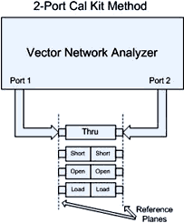
The Spectrum Analyzer is a frequency discriminating detector that detects the voltage for the signal. It will give the amplitude of signal as a function of frequency. It is scalar in measurement dimension magnitude vs. frequency. Displayed units are typically expressed in units of power (dBm). The Vector Network Analyzer measures complex magnitude and angle of RF signals vs. frequency. By using reference signals to calibrate the test system response and setting up a reference frame for the measurements, the instrument can measure the amplitude and phase angle of the AC-RF signal for each frequency it is tuned to. Displayed units are typically expressed as s-Parameters. The Vector Signal Analyzer is like a cross between a Spectrum and Network Analyzer. It also measures the signal modulation and a number of features about the modulation format and data. It measures in voltage and is in complex or scalar format depending on the data being displayed; i.e., the RF signal characteristics or the modulation format and data. Calibration S-Parameters calibration is a process of making measurements with metrology-quality calibrations standards and then applying formulas to compute the correction factors from the measurement of those standards, which determine a reference plane for subsequent measurements. A reference plane is an imaginary point of reference for the measurements being made. It defines the physical points to which the network analyzer is calibrated to have 0 dB magnitude and 0 degrees phase response. It is also the input and output planes to which reflection and transmission measurements are referenced since phase is measured relative to a specific point in the signal path. There are numerous methods and standards for Coaxial, Waveguide, Planar, probe and other interconnections methods. There are also numerous test fixtures and calibration techniques available to help the test engineer make measurements in fixtures and give them the ability to de-embed fixture components to get at the raw device or subsystem S-Parameters that are difficult or nearly impossible to measure with standard equipment (e.g. mixed impedances and more). Some of the most often used calibrations methods are: SOLT Short, Open, Load and Thru is the SOLT cal. These are physically and electrically (in terms of phase length) near identical components. The connectors and the calibration component physical parts are constructed to tolerances of 10,000ths of an inch. There are calibration parameters that help define and reference these standards. Some of these are the Open Capacitance frequency response C0, C1, C2, C3 and Short inductance frequency response L0, L1, L2 and L3 that are the coefficients for the 3rd order polynomial formulas use to correct the phase for fringe capacitance and inductance that can cause ripple in the frequency . There is the delay or electrical length for each of the parts, for the Short, Open and the Thru. The Load has an indeterminate phase due to the small signal level, so it is of no consequence. The Thru standard loss and phase shift can be calculated and removed from the measurement. What this does is shift the reference plane from the middle of the Thru and ends of the Short, Open and Load back to the instrument's or fixture's connector ground ring as the plane of reference for phase and. If no lengths and losses are specified, the calibration is less accurate and the measurement reference 0 dB, 0 degree position is more difficult to determine. In that case it is usually assumed to be in the middle of the connection Thru and ends of the Open/Short. SOLT Waveguide standards have many issues and are difficult to implement. SOLT on-wafer cal kits suffer from variation of resist implants and loss of impedance accuracy of the loads also variation of substrate dielectric constant varies the component line or system impedances. TRL Thru, Reflect, Line(s) is the TRL cal, and uses those three standards for calibration. This means that fixture effects of measurements of devices can be better removed from the device measurement, allowing better device characterization. TRL calibration requires a line of minimum length, reflections of shorts to both input and output ports and finally a Line longer than the Thru. The Line must also meet other requirements for length. Several drawbacks with TRL, among them are the separation that contacts have to undergo to accommodate the Line calibration standard, and on some substrate materials like GaAs the lines become more reactive at low frequencies due to tangent loss and so system impedance is more difficult to determine. With the LRM calibration (see below), the loads are measured for DC Resistance, which can be entered into the calibration standards to offset the VNA measurement System Zo (reference impedance). This accommodates the actual measured load impedance. The S-parameters are relative to the System Zo, as we will see later when we discuss converting S-Parameters to Arbitrary Impedance. LRM Line, Reflect, Match, or LRM, is actually a variant of TRL. When you have an infinitely long transmission line, this looks to the source just like a perfect load because there is no terminating end point to reflect any energy of the signal and it dissipates thru transmission loss. Load replacement allows the calibration to be performed in a fixture, on-wafer, in coaxial line, or on a planar substrate that does not have to be further separated. It can be done in a fixed length fixture. This and the fixed load standards can determine the System Zo at all frequencies with better accuracy, verses the issue with high tangent loss affecting low frequency measurements when using the TRL calibration It is a big advantage for On-Wafer measurements, since the test probes now do not have to have extra motion and alignment to calibrate. Waveguide calibrations are difficult to make with SOLT, but relatively easy and accurate for TRL or LRM within waveguide band restrictions. Electronic Load/Line For coaxial measurements, ATN Microwave years ago developed an electronic line/load for calibration. Agilent bought the company and now offers the electronic calibration gear to do the calibration with one connection and simple steps. It uses PIN diodes under automated control to vary the line and reflection parameters of the calibration standard electronically. This is not dependent on physical dimension variation as the mechanical standards are. They can be repeatedly measured and used with little loss of calibration accuracy. Measurements Vector network analyzer measurements are made either to coaxial connected devices or to devices with some form of fixture or ‘launch' to the device under test. The methods used to measure and calibrate or de-embed with depend on factors such as cost, equipment availability and capability. If the measurement features are not available on your version of network analyzer, then software extensions can often add to that capability at a low cost related to hardware costs. The type of fixture as well as the capabilities of the instrument may also determine which calibration and fixturing methods are available to the user. Test Fixturing
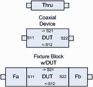
Figure 1 - Test Device and Fixtures
Figure 2 - VNA Response Calibration
Figure 3 - VNA w/ Cal Kit Calibration
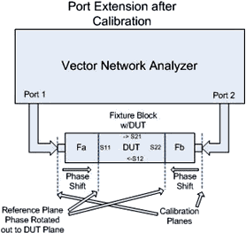
Figure 4 - VNA Fixture Measurement Using Port Extension Correction
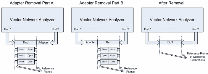
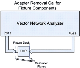
Figure 5 - VNA Adapter Removal Method of Correction
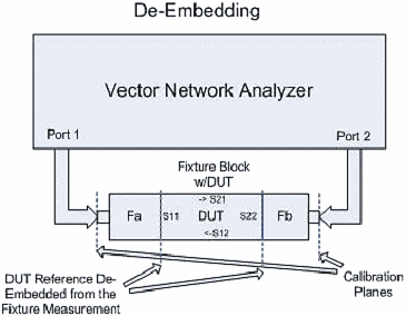
Figure 6 - VNA Fixture Measurement w/Adapter Removal
Figure 7 - VNA De-Embedding DUT from Fixture Tests fixtures are used to measure a device that does not connect to a measurement instrument directly. The device might be substrate mounted and wire bonded to microstrip that then connects to a coaxial connector in the fixture header block. See Figure 1. Response or First-Order Corrections By measuring a Thru calibration adapter with a response Thru for transmission measurements, the Thru adapter and the phase length and loss is part of the device measurement. You will then see the S21 and S11 and converse S12 and S22 measurement to be 0 dB Magnitude and 0 Degrees phase, so the Thru adapter has become part of the measurement. I always assumed the reference plane for this was basically the center of the Thru adapter. So, when measuring a coaxial device the reference plane (0 dB, 0 Deg point) is moved from the ground plane of the connection to the same position inside the device under test. See Figure 2. Cal Kit Definitions By using a fully characterized calibration kit (Cal Kit), the Cal Kit calibration coefficients are used to accurately model the calibration component magnitude and phase responses. This means they can be de-embedded from the measurement. Consider the typically used 3.5 mm Cal Kit. After calibrating, the Thru response has been removed. What that means is with the Thru still connected to the VNA after calibration, you will now not see 0 dB magnitude and 0 degrees phase. You will see the loss and phase length of the Thru cal component. The calibration has shifted the reference plane back from the middle of the connection to the ground reference plane of the coaxial connectors on both sides or on the connection planes of the probes on a planar substrate being measured. See figure 3. Port Extensions w/Simple Loss Correction The VNA allows the user to either set a phase shift for each of the ports or port extension can be set for ports 1 and/or 2 instead. The port extension method is easier, as each port extension gives both the reflection and transmission phase shift, verses the user having to set four S-parameter phase shifts. With port extensions only port 1 and 2 port extension data are entered. The S-parameters phase shift is unity for the transmission (S21) and reverse transmission (S12). The phase shift for reflections is double the transmission phase shift as the signal goes to the reference point and reflects back, thus double the length or shift. The insertion loss of the fixture is determined by Thru measurements and is divided in half and applied to the input and output of the device to correct the S21, S12, S11 and S22 magnitudes. Again, the fixture losses and phase shifts are singular for S12 and S21 and double that for S11 and S22. This is a simple first-order de-embedding or error correction method shown in Figure 4. Adapter Removal There is a mixed adapter mode where Port 1 is different from Port 2. Each of the ports has its own standards, and the calibration from each port calibration and the combined Thrus gives a hybrid calibration for these mixed adapter measurements, say for instance coaxial on one side and on-wafer on the other, or a 3.5mm female coaxial connector on one side to 7 mm on the other. This can also be used to measure a coaxial-to-probe or coaxial-to-pin on a test fixture or a wafer probe set. The female-to-female or male- to-male is referred to as “non-insertable' because they are not directly connectable without using an adapter. See Figure 5. An insertable device is a male-to-female connection or direct connection. De-Embedding In this method all components are measured for S-parameters and the adapters or fixture responses are removed mathematically from the combined response measurement. See Figures 6 and 7 for test setups. Older vector network analyzers (VNA) used a step recovery diode driven by a square wave at 21.78 MHz to generate a harmonic comb that was used for the down conversion in its wideband measurement system. Those old system architectures were susceptible to spurious and harmonic signal lock-on where the phase locked loop (PLL) could chose the wrong harmonic component for reference. Today they use direct conversion techniques that are less prone to erroneous harmonic and spurious signals. This also gives the new analyzers tuned receiver capability. Modern VNAs can measure intermodulation distortion (IMD) or harmonic components and measure active IMD or harmonic sweeps. The new Agilent PXA helps with non-linear extension S-parameters or X-parameters™, which opens up some really new measurement and device modeling capability. The newer VNAs have techniques to allow full real de-embedding of external test fixtures and the ability to measure S-parameters in mixed impedance environments. This allows measurement of a device designed with a 75 ohm reference impedance (Zo) with a VNA that has a 50 ohm system Zo. My Labview S-parameter library will help fill this gap in instrument capability on the older VNA test systems. Conclusion We showed that S-parameters can be used for a number of network computations that can add value to measurements where the equipment is limited in features. The reader can find these equations and more in my S-Parameter Library (DLL & LLB) and RFCalculator™ products (see website below). References LinkedIn: Joe Cahak See RF Calculator and soon Labview S-Parameter Library https://en.wikipedia.org/wiki/Two-port_network https://en.wikipedia.org/wiki/S-parameters https://en.wikipedia.org/wiki/ABCD-parameters#ABCD-parameters https://en.wikipedia.org/wiki/Transmission_line https://en.wikipedia.org/wiki/Reflection_coefficient https://en.wikipedia.org/wiki/Standing_wave_ratio https://en.wikipedia.org/wiki/Electrical_impedance https://en.wikipedia.org/wiki/Admittance https://en.wikipedia.org/wiki/Two-port_network#Hybrid_parameters_.28h-parameters.29 https://en.wikipedia.org/wiki/X-parameters Making S-Parameter measurements in Mixed Impedances, Jim Hillstrom, Microwaves & RF, January 1992 Agilent PN 8720-2, In-fixture Microstrip Device Measurements Using TRL* Calibration, Product Note Agilent PN 8510-5A, Specifying Calibration Standards for the Agilent 8510 Agilent 8510-13, Measuring Noninsertable Devices, Product Note Agilent AN 1287-1, Understanding the Fundamental Principles of Vector Network Analysis, Application Note Agilent AN 1287-3, Applying Error Correction to Network Analyzer Measurements, Application Note Agilent Application Note 1287-7, Improving Network Analyzer Measurements of Frequency-translating Devices Agilent AN 1287-6, Using a Network Analyzer to Characterize High-Power Components, Application Note Agilent AN 1287-9, In-Fixture Measurements Using Vector Network Analyzers, Application Note Agilent AN 1364-1, De-embedding and Embedding S-Parameter Networks Using a Vector Network Analyzer Agilent DE-EMBEDDED MEASUREMENTS USING THE HP 8510 MICROWAVE NETWORK ANALYZER Agilent Network Analyzer Basics Agilent 5989-5765EN Agilent Signal Integrity Analysis Series Part 3: The ABCs of De-Embedding Application Note Agilent AN 154, S-Parameter Design, Application Note Agilent AN 95-1 S-Parameter Techniques for Faster more accurate Network Design Microwave Engineering, David M. Pozar, Wiley, ISBN 9971-51-263-7 Networks and Systems, D Roy Choudhury, Wiley, ISBN 0-470-20867-8 Fields and Waves in Communications Electronics, Ramo, Whinnery & Van Duzer, Wiley, ISBN Lib Congress Catalog 65-19477 High-Frequency Circuit Design and measurements, Peter Yip, Chapman and hall, 0-442-31185-0 Sunshine Design Engineering Services is located in the sunny San Vicente Valley near San Diego, CA, gateway to the mountains and skies. Are you looking for new things to design, program or create and need assistance? I offer design services with specialties in electronic hardware, CAD and software engineering, and 25 years of experience with Test Engineering services in RF/microwave, transceiver and semiconductor parametric test, test application program development, automation programs, database programming, graphics and analysis, and mathematical algorithms. See also: - Noise and Noise Measurements - Measuring Semiconductor Device Input Parameters with Vector Analysis - Computing with Scattering Parameters - Measurements with Scattering Parameters - Ponderings on Power Measurements - Scattered Thoughts on Scattering Parameters Sunshine Design Engineering Services 23517 Carmena Rd Ramona, CA 92065 760-685-1126 Featuring: Test Automation Services, RF Calculator and S-Parameter Library (DLL & LLB)
Posted June 16, 2020 |